This article is more than 1 year old
Intel outs 'Poulson' speeds and feeds
Yes, more chip porn!
ISSCC Intel has released some additional about its future eight-core "Poulson" Itanium processors.
The Poulson chips are the first Itaniums to have a new microarchitecture and core redesign since the "McKinley" cores a decade ago. As previously reported, the processor has a total of 3.1 billion transistors and is implemented in Intel's current 32 nanometer wafer baking technologies, which includes strained silicon.
The Poulson chip is 18.2 by 29.9 millimeters (544 square millimeters) and has about 20 per cent less die area than the quad-core "Tukwila" Itanium 9300 chip it will eventually replace in the lineup probably in early 2012 if Intel can stick to the two-year cadence is it trying to set for the Itaniums so Hewlett-Packard, the last big user of the Itanium chips, can keep pace with Power and Sparc upgrades.
El Reg was missing a whole bunch of information about the Poulson chip when Intel gave prebriefings ahead of the ISSCC event, but Reid Riedlinger, the chief chip engineer for the processor, filled in some gaps in his presentation at ISCCC. For one thing, Riedlinger's presentation had die shots that showed a lot of the salient features of the processor, which Intel did not provide in its briefings to the press.
So, here is what the Poulson chip looks like:
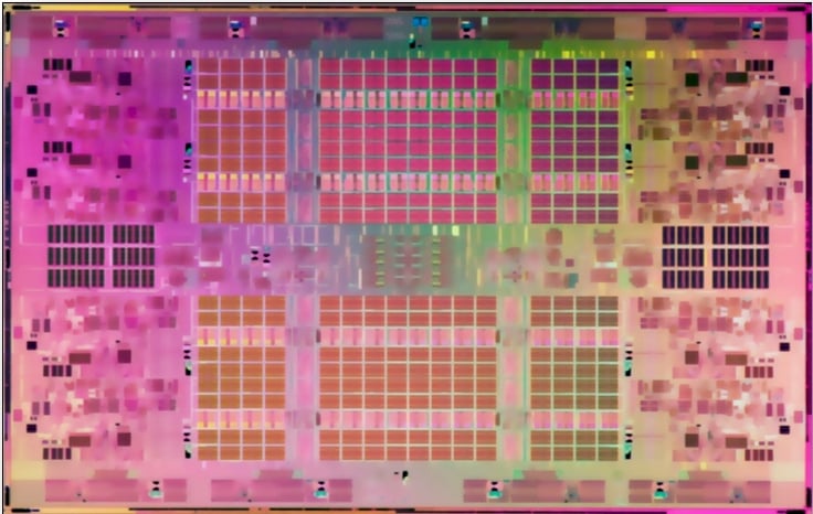
Intel's future "Poulson" Itanium processor (click to enlarge)
Like the future "Sandy Bridge-EP" and "Westmere-EX" Xeon processors from Intel, which El Reg told you all about here from ISSCC, the Poulson Itanium chip is a "cores-out" design, which means that the cores are on the outside of the chip with the shared L3 caches occupying the center of the chip.
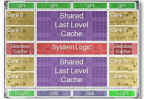
The QuickPath Interconnect (QPI), which allows point-to-point communication between processors in adjacent sockets in a system board and across multiple systems boards in an SMP server, run along the top, and the Scalable Memory Interconnect (SMI) DDR3 memory controllers and buses run along the bottom. Here's a slightly better Poulson chip schematic than Intel was handing out in its prebriefs:
Riedlinger gave out the transistor budget for the Poulson chip, which was interesting. About 712 million of those transistors are for the cores themselves, with the remaining 2.44 billion going for the uncore portions. Most of that is, as you can see from the chip shot, used up in the shared L3 cache, which is segmented in 4 MB blocks (one per core) and linked together by a high-speed, bi-directional ring interconnect.
Riedlinger said that the core logic's 712 million transitors took up about 158 square millimeters of area, ran at between 0.85 and 1.2 volts, and burns about 95 watts. The L3 caches had 2.17 billion transistors, ran at between 0.9 and 1`.1 volts, but only burned 5 watts; the L3 caches occupied 163 square millimeters of chip real estate. The system interconnect circuits linking the cores to the L3 caches on the chip were fashioned from 22 million transistors, ate up 137 square millimeters of space, ran at the same 0.9 to 1.1 volts, but burned 50 watts. The I/O logic (QPI, memory controllers, and SMI buses) were etched with the final 44 million transistors, ate 68 square millimeters of chip area, ran at 1.05 to 1.1 voltage, and slurped 20 watts under load.
The Poulson chip has a total of 54 MB of SRAM memory on it. This includes 32 MB of L3 cache, 2 MB of total L2 data cache, 4 MB of total L2 instruction cache, 2.2 MB of director cache, 3.6 MB of last level tags, and a tiny slice (169 KB) of L2 instruction tags. Don't forget the L1 data and instruction caches on each core.
