This article is more than 1 year old
Peering closer at 3D XPoint memory: What are Intel, Micron up to?
A memory crossing point, yes – but a Rubicon?
Analysis Asking what we know about Intel/Micron's XPoint memory announced yesterday is maybe the wrong question. What don't we know about it?
Here are a few mysteries:
- Is the technology patented?
- Have developers kept quiet for 10 years?
- What is the memory cell material?
- What is their selector material?
- What is the process used to switch the memory cell's resistance by applying voltage?
- What is the cell geometry size?
- How many dies can be cut from a 300mm wafer?
- What is the switching time for reads and writes?
- Why are there two layers and not three or four?
- What is the die footprint?
It would be astonishing if the technology isn't ringed with patents. We also think it is highly unlikely that either Intel or Micron discovered the memory cell material with original research. It's more likely that one or the other has licensed or otherwise acquired existing technology.
Another thought is that information about the technology must have been revealed, deliberately or inadvertently, by the hundred or more people involved with it over the past few years. It's a case of knowing where to look.
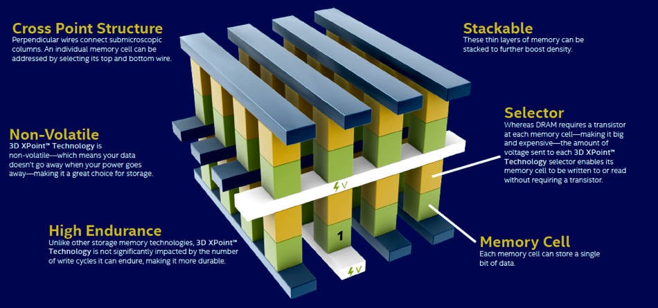
3D Point memory infographic. Click image for bigger version
An infographic about 3D XPoint memory said it delivered ten times more performance than NAND across a PCIe NVMe interface.
Intel and Micron said 3D XPoint memory was up to 1,000 times faster than flash. Here is a diagram they showed to illustrate this:
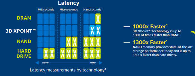
XPoint latency diagram
We can see that XPoint is hundreds of times faster than flash, with 1,000x being a probable extreme case.
