This article is more than 1 year old
Intel CEO waves around 22nm wafer
Still an 'immature' process, though
IDF Intel CEO Paul Otellini today showed off a 300mm wafer of memory arrays fabbed at 22nm and reiterated the chip giant's plan to release microprocessors produced at that node in 2011.
As yet, Intel hasn't named its first 22nm CPU, but if the company follows its "tick-tock" regular release programme, the chip will go into production just over a year from now as a die-shrink of next year's 32nm 'Sandy Bridge' architecture.

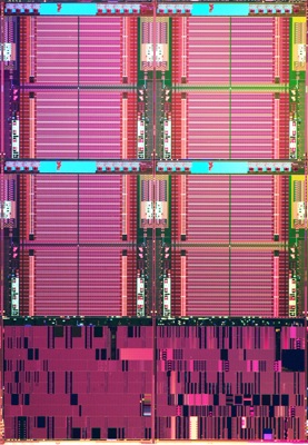
Testing the process: Intel's 22nm SRAM chip
Otellini claimed "significant" work has been done on the 22nm incarnation of Sandy Bridge. It will use the third generation of Intel's high-k metal gate transistor tech, which is a key element of what the wafer of memory chips is designed to test.
Otellini said the arrays within the wafer - each die containing 364m transistors of the kinds that will be used in the subsequent CPU, along with processor-oriented I/O circuitry too - work and thus show that the 22nm production process - called 'P1270' for CPUs and 'P1271' for Atom-branded system-on-a-chip products - is on track.
Which is all he said - neither Otellini nor other Intel executives when questioned would go into any technical details about those transistors themselves.
Indeed, Mark Bohr, an Intel Senior Fellow and its Director of Process Architecture and Integration, described P1270 as an "immature process", admitting that there's still a lot of work to be done to get it ready to punch out production processors. That work will take up most of the coming year or so. ®
