This article is more than 1 year old
Nvidia fires off Fermi, pledges radical new GPUs
Three billion-transistor HPC chip, anyone?
Nvidia last night introduced the new GPU design that will feed into its next-generation GeForce graphics chips and Tesla GPGPU offerings but which the company also hopes will drive it ever deeper into general number crunching.
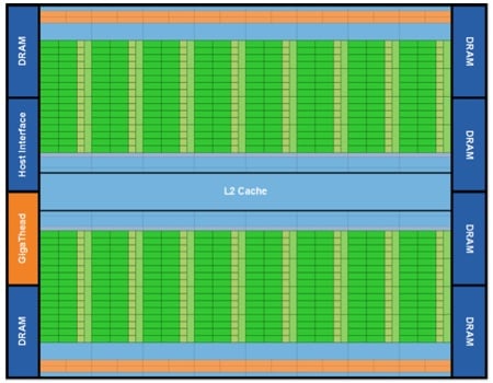
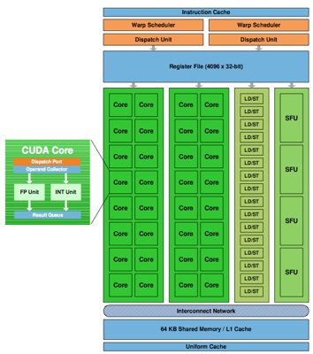
While the new chip is dubbed 'Fermi', so is the architecture that connects a multitude of what Nvidia calls a "Streaming Multiprocessor". The SM design the company outlined yesterday contains 32 basic Cuda cores - four times as many found in previous generations of SM - each comprising one integer and one floating-point maths unit. It is able to schedule two groups of 32 threads - a group Nvidia calls a "warp" - at once.

Nvidia's Fermi: each of the 16 green strips is...
The networked cores connect to 64KB of shared L1 cache, also used by four Special Function Units (SFUs) which handle complex maths formulae such as sines and cosines.
Fermi itself packs in 16 SMs - that's 512 Cuda cores in total - which tap into shared 768KB L2 cache and can reach out to a maximum of 6GB of GDDR 5 memory over a 384-bit interface and with ECC support
This is only the first Firmi GPU design. It's aimed at science and engineering GPGPU apps rather than game graphics, so future Fermi-based GeForce chips will likely sport less complex layouts. GT300, Nvidia's next GPU core, will be derived from Fermi, but don't expect it to show off all the superlatives Nvidia has been claiming for the Fermi chip.

...one of these 32-core Stream Multiprocessors
The first Fermi design uses three billion transistors. It supports 64-bit addressing, double that of the previous generation GT200 architecture, the one used in GeForce GTX 200-series GPUs. It can handle 256 double-precision floating point ops per clock and 512 single-precision ops, up from GT200's 30 and 240, respectively.
And the key fact Nvidia didn't mention: when the Fermi-sourced GeForces will go on sale. ®
