This article is more than 1 year old
IBM shows off Power7 HPC monster
Big Blue unveils big box: Crowd goes wild
SC09 IBM likes to go on and on about the transaction processing power and I/O bandwidth of its System z mainframes, but now there is a new and much bigger kid on the block.
Its name is the Power Systems IH supercomputing node, based on the company's forthcoming Power7 processors and a new homegrown switching system that blends optical and copper interconnects.
The Power7 IH node was on display at the SC09 supercomputer trade show last week in Portland, Oregon, and El Reg was on hand to get the scoop from the techies who designed the iron. This server node is the heart of the 1 petaflop "Blue Waters" supercomputer being installed at the University of Illinois. (That's sustained, not peak, performance.)
As we have previously reported, IBM lifted the veil a bit on its Power7 family of chips and chip packages at the Hot Chips conference in August. The Power7 chips are implemented in a 45 nanometer copper/SOI process and have 1.2 billion transistors with eight cores on a single die.
Each Power7 core has 12 execution units: two fixed point units, two load store units, four double-precision floating point units, one vector unit (for doing matrix maths), and one decimal floating point unit (for doing money maths). Those floating point units, like those in all past generations of 64-bit Power processors that trace their heritage back to IBM's AS/400 designs from 1995 (not the crappy PowerPC chips that came out of the IBM-Motorola-Apple partnership) can do two floating point operations per clock cycle.
The Power7 core has 32 KB of L1 instruction cache and 32 KB of L1 data cache. Each core sports simultaneous multithreading that delivers four virtual threads per core, and has a 256 KB of L2 cache tightly coupled to it. The chip also has 32 MB of embedded DRAM that acts as a shared L3 cache, with 4 MB segments affiliated with each of the eight cores. The Power7 chip has two dual-channel DDR3 memory controllers implemented on the chip, which deliver 100 GB/sec of sustained bandwidth per chip.

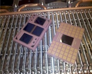
The Power7 IH four-chip package and its companion switch
with mixed optical/copper interconnect
At SC09, IBM gave out a lot more details on the four-chip multichip module (MCM) that it said it was cooking up for supercomputing customers - and by the way, the Power7 IH server node is a lot denser, in terms of flops per unit volume, than anyone had been led to believe. The picture at the left shows the Power7 IH node MCM chip package, with the four eight-core Power7 chips. Next to it is the IH node hub/switch, which is implemented in a similar chip package.
Both chip packages have the same pin count at 5,336 pins (92 pins by 58 pins), according to Alan Benner, a senior technical staff member of the server and network architecture team within IBM's Systems and Technology Group: more on this hub/switch in a minute. The package has 512 GB/sec of aggregate memory bandwidth and 192 GB/sec of I/O bandwidth.
