This article is more than 1 year old
IBM's BlueGene/Q super chip grows 18th core
It's nice to have a spare
Hot Chips The mystery surrounding the number of cores in the 64-bit Power processor that will be at the heart of the 20 petaflops "Sequoia" BlueGene/Q supercomputer has been finally cleared up.
Back at the SC10 supercomputing conference in November 2010, a software engineer working on the BlueGene/Q system told El Reg that the processor module at the heart of the system would have 17 cores: one to run the Linux kernel and the 16 others to perform mathematical calculations. IBM also said at the time that this chip would be a variant of the PowerA2 "wirespeed" processor, but geared down to 1.6GHz from its 2.3GHz design speed.
In February 2011, when Argonne National Laboratory said that it was going to take a 10 petaflop super based on the BlueGene/Q design (basically half of the Sequoia machine that is going into Lawrence Livermore National Laboratory), IBM told El Reg that it was just a 16-core chip, nothing funky.
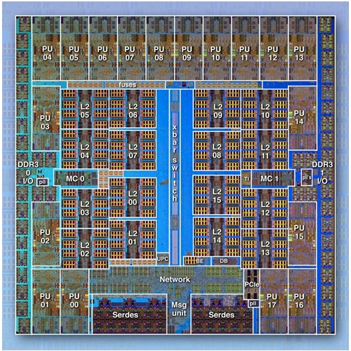
For whatever reason, neither turns out to be true. The BlueGene/Q processor, the company revealed at the Hot Chips conference at Stanford University late last week, actually has 18 cores: 16 cores for doing work, one core for running Linux services, and a spare that is intended to merely increase the yield that IBM Microelectronics can get out of its chip fabs but which can, according to George Chiu, senior manager of advanced high performance systems at IBM, be activated and used in the system, in theory.
Chiu was very clear, however, that he was not making any promises that this 18th core would be used as a hot spare in any BlueGene/Q supers, but merely that the capability is there.
Big Blue detail
IBM gave out a lot more detail on the BlueGene/Q processor at Hot Chips, and Chiu walked El Reg through the details. The chip looks like this:

The BlueGene/Q custom Power processor
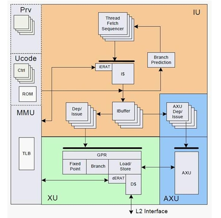
Like other processor designs these days, the BlueGene/Q processor is an example of a system-on-a-chip design, which tries to cram as many components of the system board onto the chip. The BlueGeneQ processor is based on the Power A2 core that IBM created for networking devices and experimentation, and this is the block diagram of the core:

The BlueGene/Q processor's Power A2 core block diagram
This Power A2 core has a 64-bit instruction set, like other commercial Power-based processors sold by IBM since 1995 but unlike the prior 32-bit PowerPC chips used in prior BlueGene/L and BlueGene/P supercomputers. The A2 core have four threads and has in-order dispatch, execution, and completion instead of out-of-order execution common in many RISC processor designs. The A2 core has 16KB of L1 data cache and another 16KB of L1 instruction cache. Each core also includes a quad-pumped double-precision floating point unit, which is blocked out thus:

The quad-pumped FPU in each BlueGene/Q core
Each FPU on each core has four pipelines, which can be used to execute scalar floating point instructions, four-wide SIMD instructions, or two-wide complex arithmetic SIMD instructions. These instructions are extensions of the of the Power instruction set. The FPU has a six-stage pipeline and has permute instructions to reorganize vector data on the fly; it can do a maximum of eight concurrent floating point operations per clock plus a load and a store.
Crossbar connection
At the heart of the BlueGene/Q chip is a crossbar switch, which links the cores and L2 cache memory together. This crossbar runs at half the clock frequency, at 800MHz, and it has a peak bisection bandwidth of 563GB/sec. It connects the processors, the L2 cache segments, the networking logic, and other parts of the chip together.
Like IBM's commercial Power7 chip, the BlueGene/Q processor has 32MB of embedded DRAM as cache memory, but this is implemented as an L3 cache on the Power7 and it's an L2 cache on the BlueGene/Q processors. Each BlueGene/Q chip has two DDR3 memory controllers, which have ECC scrubbing and which support 16GB of total memory running at 1.33GHz.
These memory controllers interface with eight slices of L2 cache, handling their cache misses (one controllers for each half of the 16 cores on the chip). The DDR3 memory and the BlueGene/Q chips are soldered onto the same processor card, and the two memory controllers provide 42.7GB/sec of bandwidth from the processor out to main memory on the card.
The logic for IBM's 5D torus interconnect is also embedded on the chips, with 11 links running at 2GB/sec. Two of these can be used for PCI-Express 2.0 x8 peripheral slots. The 14-port crossbar switch/router at the center of the chip supports point-to-point, collective, and barrier messages and also implements direct memory access between nodes.
The spare
The 17th core runs Red Hat Enterprise Linux, and it's designed to offload operating system services from the other 16 working cores on the BlueGene/Q processor to eliminate distracting OS noise and jitter. This 17th core will take care of interrupt handling, asynchronous I/O, MPI pacing, and RAS event handling, which you need in a system with 1.57 million working cores. In the event of a core failure, the system can remap the cores, bringing the 18th core online if it hasn't already been blocked off because it has a booger on it.
But the 18th core was really added to increase chip yields.
The BlueGene/Q processor is 359.5 square millimeters in area (18.96 millimeters per side in an actual square), and it has around 1.47 billion transistors. It is implemented in the 45 nanometer copper/SOI process that IBM used to make the Power7 chips. The cores used in the BlueGene/Q chip will all spin at 1.6GHz, with IBM varying the voltage as necessary around its 0.8 volt target to keep that clock speed rock solid and therefore be able to synchronize events across those 1.57 million cores.
By lowering both the clock speed and voltage from the Power A2 processor, IBM is giving up some performance per chip, but it is able to dramatically lower the active and leakage power of the processor. The 16-cores are designed to deliver 204.8 gigaflops at a power draw of 55 watts.
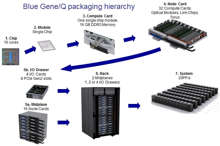
Here's how the full BlueGene/Q system gets integrated:
The compute cards and the optical interconnect modules have water blocks on them to keep them cool. The system is designed to use water at between 60 and 65 degrees Fahrenheit. The Sequoia system that Lawrence Livermore is getting will have 96 racks of BlueGene/Q nodes to reach its 20 pteaflops performance level, and it is expected to consume around 6.6 megawatts.
BlueGene/Q is expected to start shipping to Lawrence Livermore and Argonne national labs, which are financed by the US Department of Energy, next year. ®

