This article is more than 1 year old
WTF is... Intel's Ivy Bridge
Inside Core i's third generation
Feature

Intel’s latest processor architecture, codenamed Ivy Bridge, is its previous one, Sandy Bridge, shrunk. Sandy Bridge chips, marketed as second-generation Core i CPUs, were produced using a 32nm process. Ivy Bridge is 22nm
Actually, there's a little bit more to it than that.

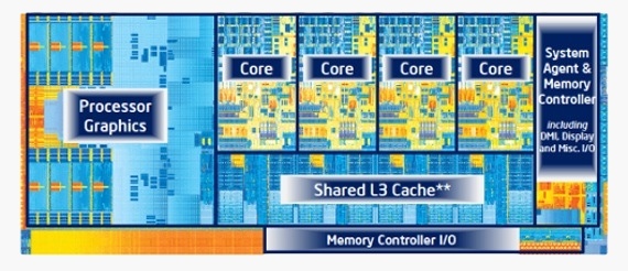
The Ivy Bridge die layout is indeed much the same as Sandy Bridge's. There are four 64-bit x86 processor cores, a memory controller and a graphics processor all integrated onto the same silicon die. Each CPU core has 64KB of Level 1 (L1) cache and 256KB of second level cache (L2) and all four cores and the graphics core share 8MB of L3 cache, called Smart Cache by Intel.
The die shrink from 32nm to 22nm allows Intel to pack in more transistors into an even smaller space. The Sandy Bridge 3.5GHz Core i7-2700K has 1.16 billion transistors on a 216mm² die. The Ivy Bridge equivalent, the i7-3770K, measures just 160mm² and contains 1.4 billion transistors - 21 per cent more.

What's new, according to Intel...

...and what is shares with Sandy Bridge
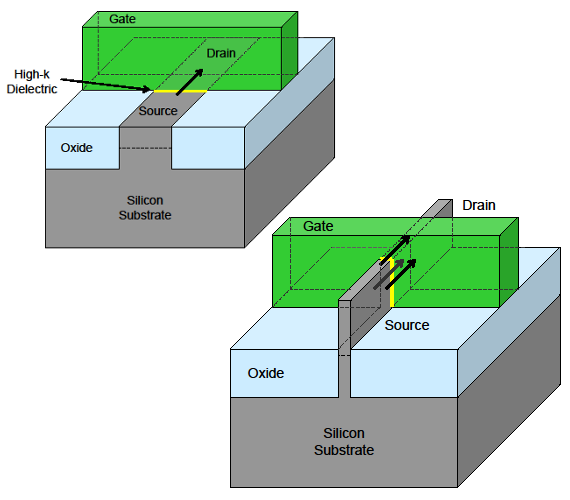
At the heart of the new fabrication process is the Intel’s Tri-Gate transistor technology, which the chip giant is calling the world’s first '3D' transistor. Traditionally, the transistors in a processor or any other silicon chip are to all intents and purposes flat, so they're considered to be 2D even though they're not literally so. The new Tri-Gate transistors have a fin that stands vertically up off the silicon substrate, hence the 3D tag.
This design helps with the real enemy of die shrinkage: electron leakage. A transistor is a switch, the on and off state determined by whether the "gate" allows current to flow from "source" to "drain".
As transistors get smaller - that 32nm and 22nm numbers the production process is named after record the size of the transistor - electrons can more easily pass through the device, even if it's turned off, thanks to the quirky properties of electrons and Quantum Mechanics.

The traditional transistor design (left) and Intel's Tri-Gate structure (right). Wrapping the gate around the 'fin' channel cuts leakage
The new Tri-Gate design essentially increases the gate's surface area, making it much better at controlling electron flow - it can turn the current on and off more quickly than the traditional design can - and at reducing electron leakage.
And it allows more transistors to be added to a smaller space, which will be very useful for manufacturing even smaller dies in the future.
