This article is more than 1 year old
Inside Nvidia's GK110 monster GPU
Fermi, Tesla, and Maxwell would all want one
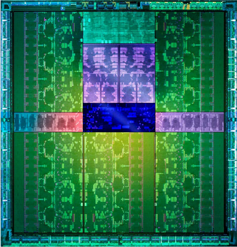
At the tail end of the GPU Technology Conference in San Jose this week, graphics chip juggernaut and compute wannabe Nvidia divulged the salient characteristics of the high-end "Kepler2" GK110 GPU chips that are going to be the foundation of the two largest supercomputers in the world and that are no doubt going to make their way into plenty of workstations and clusters in the next several years.
If you just want awesome graphics, then the dual-chip GTX 690 graphics card, which is based on the smaller "Kepler1" GK104 GPU chip, which Nvidia previewed back in March, is what you want. And if you want to do single-precision floating point math like mad, then the Tesla K10 coprocessor, also sporting two GK104 chips, is what you need to do your image processing, signal processing, seismic processing, or chemical modeling inside of server clusters.
But if you want to use GPU coprocessors to boost the performance of computational fluid dynamics, finite element analysis, financial calculations, and physics simulations workloads that depend heavily on double-precision floating point math, then you are going to have to wait until October or November for Nvidia to start shipping its "Kepler2" GK110 GPUs.
This chip is a monster, weighing in at a staggering 7.1 billion transistors, but it will have three times the floating point performance of the top-end "Fermi" GF110 chip it replaces, which has a peak rating of 665 gigaflops at double precision spinning at 1.3GHz.
This is much better performance increase than you would expect from Moore's Law alone, and obviously Nvidia has been able to get there through a combination of a radically different GPU design, a process shrink from 40 nanometers down to 28 nanometers (which allows for lower power consumption on transistors and therefore more transistors in a given area), and a much larger chip.
Nvidia has not released all of the feeds and speeds on the new GK104 and GK110 GPUs, such as clock speeds and precise thermals for the Tesla K10 and K20 cards that deploy them respectively. The chips are alike in some ways and very different in others.
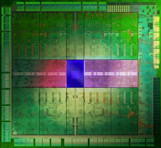
On the Kepler1 GK104 chip, Nvidia has a streaming multiprocessor extreme (SMX) unit of processing in the GPU, which has 192 single-precision CUDA cores lumped into a streaming multiprocessor group. Eight of these SMX units are on a single GPU chip for a total of 1,536 cores. As with the Fermi GPUs, the Kepler1 design put a 64KB L1 cache at the disposal of the streaming multiprocessor collective and then added a 768KB L2 cache that is shared across all of the streaming multiprocessors on the unit.
With the Fermis, there had 32 CUDA cores in an SM unit, and with the Keplers, you have 192 cores in an SMX unit. You have many more cores in the Keplers, but they run considerably slower on the order of 1GHz for the Kepler1 chip on the GK104 unit running on the GTX 680 single-unit graphics card. Nvidia is being cagey about the clock speed on the Kepler1 and Kepler2 chips used in the Tesla K10 and K20 server and workstation coprocessors.
The GK104 chip has 3.54 billion transistors that etch a total of eight of these SMX units, which have 1,536 cores. The GK104 has six memory controllers on the die, just like its Fermi predecessor, and the same 64KB of L1 cache for the SMX units and 768MB of L2 cache shared by all of the SMX units, but it also adds a 48KB read-only cache memory that is tied to the texture units on the GPU that can also be used as a cache for the SMX units.
Nvidia says that a single GK104 chip in the Tesla K10 coprocessor card will deliver a peak 2.29 teraflops of single-precision oomph and a tiny 95 gigaflops of double-precision number-crunching power. El Reg spoke to Jonah Alben, senior vice president of GPU engineering at Nvidia, who said the Tesla K10 card puts two of these GK104 chips units on a single card with 8GB of GDDR5 main memory and fits into the same 225 watt thermal envelope as the Tesla M2090 coprocessor card it replaces. Alben would not tell us the clock speed on the GK104 used in the Tesla K10, and Nvidia has been very careful not to out put SP and DP figures for the GeForce cards using the same chips to make it hard to make comparisons.
If you assume two single-precision calculations per clock in the modified CUDA cores and that all 1,536 cores are active on the GK104 in the Tesla K10, then it runs at 745MHz. If some of the cores are deactivated (as was the case with the original Fermi chips used in the Tesla coprocessors, which had only 448 of their total 512 cores on), then the clock speed will be higher in inverse proportion to the number of active cores relative to total possible cores. If you assume that the same ratio of cores are duds as with the Fermis, then you are talking about having 1,344 cores active in the two GK110s running in the Tesla K10 coprocessor at a clock speed of 852MHz.
By comparison, the GeForce GTX 680 graphics card announced in March weighs in at 195 watts with the 1,536 CUDA cores all active in its one GK104 chip running at 1,006MHz (1,058MHz turbo boost) and 2GB of GDDR5 memory. The dual-GPU GTX 690 graphics card has two GK104 chips running at 915MHz (1,019MHz turbo boost) plus 4GB of GDDR5 memory and emits 300 watts of heat as it runs at peak.


