This article is more than 1 year old
Inside Nvidia's GK110 monster GPU
Fermi, Tesla, and Maxwell would all want one
With the Kepler2 GK110 chip, Nvidia is doing a bunch of different things to make the GPU better at double precision workloads and easier to program for the kinds of workloads that the company expects to be deployed in modern supercomputers. For one thing, those neat Hyper-Q and Dynamic Parallelism features that make the Kepler GPUs wildly more efficient and easier to program are only available in the GK110 chip. (Sorry GK104 buyers.) Also, the GK104 has ECC scrubbing on the GDDR5 memory, but the GK110 has it on the cache memory and cores as well, according to Alben.
A chip off the old block
Here's what the block diagram of the Kepler2 GK110 chip, which has 7.1 billion transistors, looks like:
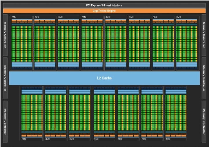
Block diagram of Nvidia's 'Kepler2' GK110 GPU chip (click to enlarge)
As you can see, the chip has 15 SMX units, but Nvidia says that different models of the chip could ship with only 13 or 14 SMX units activated. Similarly, it seems very unlikely that all of the cores will be working in the initial GK110 shipments, just as they were not all working in the Fermi GF110 chips uses in the Tesla M2050s and M2070s. The GK110 has 64KB of L1 cache for each SMX, plus that special 48KB texture unit memory that can be used as a read-only cache now, too.

Nvidia's "Kepler2" GK110 SMX block
diagram (click to enlarge)
The GK110 chip has twice as much L2 cache memory across the SMX units as the GK104 – at 1.5MB – and this is also twice the capacity the Fermi line of GF104 and GF110 chips used in the Tesla coprocessors had. The bandwidth on the L2 cache is also twice as high on the Kepler2 compared to the Fermi chips. The overhead of using ECC scrubbing has been reduced by 66 per cent on a variety of internal Nvidia benchmark tests compared to turning it off and not having any performance hit on memory and no ECC protection (which is bad for certain kinds of systems and their applications).
The SMX unit in the Kepler2 GK110 chip has 192 single-precision CUDA cores, but adds in 64 double-precision floating point units. The prior Fermi GF110 had 512 cores (with DP units tacked onto each SP core) and ran at 1.3GHz to deliver 665 gigaflops of DP oomph in a 225 watt thermal envelope with 6GB of GDDR5 memory. It could deliver a double precision flop for every two clocks with all those 512 cores fired up. The GK110 has 960 DP units linked to its total of 2,880 CUDA cores, as you can see from the SMX block diagram. With the Fermi chips, you paired an integer (ALU) and a floating point (FP) unit in the core, which could do 256 fused multiply-add (FMA) operations per clock across those 512 cores at double precision or 512 FMAs per clock in single precision.
It is not entirely clear to El Reg how this different balance of CUDA cores (presumably with integrated FP units as before) and external DP units will play out, or what performance it might yield. In some documents and presentations, Nvidia has said that the Kepler2 chip will yield three times the performance per watt of the Fermi chip it replaces (the GF110 used in the Tesla M2090 card). In other cases it says it will deliver three times the performance, and yet still at other times it says merely that performance will be greater than 1 teraflops for the card. Well, as for the latter, it had better be.
But let's have some fun. At 600MHz and assuming those internal DP units in the CUDA cores can do one-half DP FMA operation per clock as on the Fermis, you are at 864 gigaflops across those 2,880 CUDA cores on the full-on GK110 chip. Let's guess that those external DP units added to the they can do two DP ops per clock (why not, plenty of other FP units do?) and you add another 1.15 teraflops DP at 600MHz across those 960 external DP floating point units. Add them up, and you are at just over 2 teraflops of aggregate DP floating point oomph (against something like 3.54 teraflops single precision) and that is the magic 3X times the DP performance of the GF110 Fermi chip. As you can see, in this scenario, two GK104s running at 745MHz have about 33 per cent more SP oomph than one GK110 would have at 600MHz. Which is why you might do it that way.
And I may have totally misinterpreted how these CUDA cores and external DP units work. (It's been a long week.) It could be that the CUDA cores on the GK110 only do single precision math and the external DP units can do two DP ops per clock, and at 1GHz you would have 1.92 teraflops DP, again that magic number.
Either way, could such a chip run at anything like 225 watts with maybe 16GB of GDDR5 memory? Good question, and Nvidia is not answering yet.
What is pretty clear is that Nvidia wants to make big bucks on the Kepler2 GK110, and it is going to charge for those extra goodies like Hyper-Q and Dynamic Parallelism. It seems very unlikely that Nvidia will be charging $3,000 for this card, as it is expecting the street price for the Kepler1-based Tesla K10 will be priced based on its own giveway promotion.
Here's how the salient characteristics of the two Fermi and two Kepler chips used in the Tesla coprocessors line up against each other:
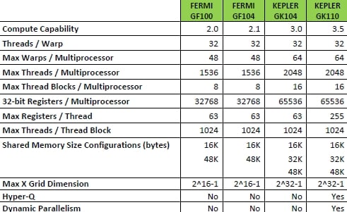
Feeds and speeds for Fermi and Kepler GPUs
As you can see, Nvidia has jacked up a whole bunch of features on the Kepler2 GK110 chip to support all the new features and boost throughput. While the thread count per SMX has not been increased that much (up 25 per cent to 2,048 threads), the maximum number of 32-bit registers per thread has been boosted from 63 to 255, which means in a lot of cases the registers will not have to spill out their contents to memory when they are juggling work. Using benchmark tests, Nvidia says that the average app running on Fermi GPU coprocessors had 110 registers per thread, so 63 just wasn't it. On one app, called Quda QCD, a quantum chromodynamics app, the registers will spilling all the time and on the GK110, it doesn't happen any more and the application is running 5.3 times faster.
The Kepler2 chip also has a new shuffle instruction, which allows threads in a group of threads called a warp (which has 32 threads) to share data, eliminating separate load-store operations. The Kepler chip also has significantly improved atomic operations, which help speed up parallel sorting and reduction operations.
The other big change is in the workflow for instructions inside the Kepler chip:

Workflow in Fermi and Kepler GPUs (click to enlarge)
The Dynamic Parallelism feature of the GK110, which allows a GPU kernel to spawn more kernels as it needs to perform nested loop or recursion functions, is enabled in part by a new grid management unit, the block diagram of which is outlined above.
And yes, you have to be careful. "You can create a fork bomb in CUDA," explained Stephen Jones, CUDA developer at Nvidia, in a keynote going over the Kepler2 details. "And just like on a Unix system, if you do that, I will tell you that it is your own fault."
To find out more about the Kepler2 GPU, see this Kepler GK110 whitepaper. ®
