This article is more than 1 year old
Applied Micro's X-Gene server chip ARMed to the teeth
Ready to take a bite out of x86 servers and Cisco
Hot Chips An opportunity to define the future of server processing comes along once every decade or so, and Applied Micro Circuit, a company known for its networking chips and PowerPC-based embedded controllers, wants to move up into the big leagues to take on Intel, Advanced Micro Devices, and the handful of remaining etchers of RISC processors for the data center.
Applied Micro may be an upstart in the server chip racket and it may be facing long odds, but Paramesh Gopi, the company's president and CEO, and Gaurav Singh, its vice president of engineering for ARM and PowerPC processors (and who worked at AMD on Athlon and Opteron processor designs), are not playing with the X-Gene ARM processor that they have created for modern, hyperscale data center workloads.
If people were skeptical about the design and deliverability of the X-Gene processor when it was announced last October, they would have been more encouraged if they had attended the Hot Chips 24 conference in Cupertino this week.
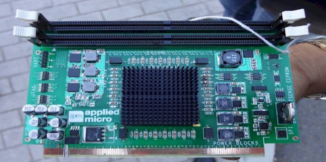
Not only did Gopi and Singh show up to talk up the X-Gene chip, but Gopi whipped out a completed X-Gene server card, ready to plug into a PCI-Express 3.0 backplane and be put to work, when he was giving his presentation on the stage.
Gopi quickly tucked it into his coat pocket and left, leaving Singh to go over the details, but El Reg chased Gopi down in the parking lot and convinced him to disobey the lawyers and show off the finished board.
The smartest thing that Hewlett-Packard, IBM, or Dell could do right now is to buy Applied Micro before it gets too expensive. And maybe AMD or Intel should do it, too.
Applied Micro has $211.3m in trailing revenues for the past four quarters, and has been hemorrhaging cash, losing a staggering $110m in large part due to its radically increased research and development expenses related to the X-Gene processor.
With a market capitalization of $335.2m right now, Applied Micro is not going to get any cheaper than it is today. It's arguably worth at least $500m and maybe even more, given all the hard work it has done to come to market with the very first 64-bit ARMv8 processor design – and one designed for profitable servers, at that.

AMCC's X-Gene server card--no longer a simulation running on an FPGAs
That said, it would be just fine for Applied Micro to enter the ranks of server chip makers all by itself, doing the designs and letting Taiwan Semiconductor Manufacturing Corp do the fabbing, just like AMD, Oracle, Nvidia, and Fujitsu, among others, do for GPUs and GPUs.
A tale of two ARM server chips
Applied Micro has given out some of the basic concepts embodied in the X-Gene ARM processor and its related processor and system interconnect, but has thus far been a bit vague about the core counts on the chip and many of the basic feeds and speeds of the processor.
Singh revealed a bunch of the specifics of the processor at Hot Chips, but plenty of the details are still to be revealed when the chip and related server boards are announced. Gopi tells El Reg that the X-Gene chip will sample to OEM customers sometime before the end of the year and that volume shipments will begin next year.

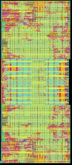
Die shot of the X-Gene ARM server processor
Calxeda. Marvell, and any other potential ARM server contenders don't have much time to come up with their own ARMv8 derivatives. Although a full-on ARM chip from Intel, IBM, or AMD would certainly cause a pause for Applied Micro.
The X-Gene chip, like the 32-bit ARM Cortex A9-derived EnergyCore processors from Calxeda, is a true system on a chip, and that server card above looks a lot smaller than it appears in the photo. (You really can put it in your sportcoat inside pocket, and El Reg was tempted to try.) That means everything but DDR3 main memory sticks and disk drives is on the chip, including a system interconnect that can lash multiple processors together over a server midplane.
A comparison with the Calxeda ECX-1000 is illustrative. Each Cortex-A9 core in the ECX-1000 chip has 32KB of L1 data cache and 32KB of L1 instruction cache each, plus a 4MB L2 cache that is shared across those four cores. These cores have an eight-stage pipeline and can do out-of-order execution as most modern processors do (even those powering IBM mainframes for the past several years).
The cores are all power gated, so they can be turned off if they are not in use. Each Cortex-A9 core runs at 1.1GHz or 1.4GHz and includes a scalar floating point unit that can do single-precision or double-precision operations, plus a NEON SIMD media processing unit that has 64-bit and 128-bit registers and that can also do floating point ops, too.
Calxeda has implemented a very fast distributed Layer 2 Ethernet switch at the heart of the EnergyCore ECX-1000 processors to let multiple sockets talk to each other as distinct server nodes. The EXC-1000s currently put up to four Cortex-A9 cores on a die, where they can share L2 cache and present a single image to an operating system as a four-threaded processor. The EnergyCore fabric switch can present Gigabit or 10 Gigabit Ethernet links to the outside world.
The ECX-1000 chips are implemented in a 40 nanometer process and baked by TSMC, just like the X-Gene chips from Applied Micro are. And like Calxeda, Applied Micro's next chips will be etched using TSMC's 28 nanometer process, which is being used by AMD and Nvidia for the current GPUs, and by AMD and Oracle for their impending CPUs.
The X-Gene processor is quite a bit different from the ECX-1000 in a number of respects, starting with the fact that it is a 64-bit design from the ground up and is based on the 64-bit ARMv8 specification announced last fall.
"ARM has really done a fine job in implementing an architecture that makes a very fine server part," Singh explained.
The 64-bitness of ARMv8 spec means it has significantly more potential memory addressability than any 32-bit or 40-bit ARMv7 variant currently on the market, and it also means that code written for 64-bit x86 or RISC processors can be more easily ported to this chip. Cramming 64-bit code back into 32 bit memory spaces is not trivial, although there are plenty of webby workloads where a 32-bit operating system and memory space will do the job. But in the long run (meaning next year), 64-bit memory addressing will be the rule for the ARM server chips.
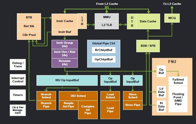
Here's what the components on the X-Gene chip look like:

Block diagram of the X-Gene ARM chip
According to Singh, the X-Gene ARMv8 derivative implemented by Applied Micro will nonetheless have full compatibility with 32-bit ARM servers, and in fact will also sport many of the CISC-like functions that have sometimes been added to 32-bit ARM processors and that are used by applications. These CISC instructions are mapped on the fly to RISC operations.
The integer unit can do two integer operations per cycle and has separate pipelines for load and store. The core also sports its own floating point/SIMD unit, which has an out-of-order scheduler that can push through one operation per cycle, plus a load and a store. The FP unit can do 128-bit processing, but since there is only one unit, it cannot be double-pumped to emulate Intel's and AMD's AVX vector math instructions. (That would be a nice feature for X-Gene 2.0.)
What we now know about X-Gene is that it uses a two-core module as the basic building block of the processor. Each core has its own L1 data and L1 instruction cache, and there is a shared L2 cache that spans these two ARM cores.
The core has a four-wide, out-of-order execution unit for integer work, and includes full virtualization support including nested page tables. This is a feature that x86 hypervisors make use of to boost the performance of virtual machines running atop hypervisors like VMware's ESXi, Citrix Systems' Xen, Red Hat's KVM, and Microsoft's Hyper-V. And it means that any of these hypervisors can be ported from x86 to X-Gene processors – and probably will be in the long run, if ARM servers take off.
The cores have dynamic voltage and frequency scaling and clock gating, and the normal C0 through C6 power states that are similar to x86 processors.
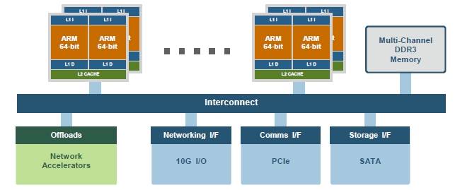
The caching architecture is a key aspect of the X-Gene chip, according to Singh. The L1 and L2 caches have hardware prefetching, and there is a "scalable modular" L3 cache, shared by all of the core modules, that sits on the data switch at the heart of the X-Gene chip. This data switch sits inline with a central snoop controller for cache memories, two memory bridges to DDR main memory, and and I/O bridge to reach out to peripherals like disk and flash drives.
Neither Singh nor Gopi would say much about this coherent network switch, but it is what links multiple modules on a die into a single system image for software. It hooks these core modules into memory and the L3 cache on the die, too, and it is also extended to be a distributed Layer 2 switch between multiple processor sockets, much like Calxeda is doing with its EnergyCore fabric.
Applied Micro would not divulge any of the sizes of the L1, L2, and L3 caches or the watts at which the chips burn.

The server on chip design of X-Gene
This coherent network runs at the full CPU clock frequency and has a 15 nanosecond latency and delivers 160GB/sec of bandwidth. It can, says Singh, manage up to 400 transactions in flight. It has interfaces to network accelerators, 10GE ports, and other PCI-Express 3.0 peripheral and SATA slots.
Gopi says that the initial X-Gene chip implemented in the 40 nanometer process will top out at four core modules and eight cores, with a maximum of 256GB of physical memory, 40GB/sec of networking I/O, and 17 lanes of PCI-Express 3.0 bandwidth to carve up into slots.
The top speed of these X-Gene cores will be a very respectable 2.5GHz, and the coherent fabric will be able to glue those four core modules together into a single system image for a Linux operating system (and maybe a Windows operating system if Microsoft gets a clue), and it will also be able to link up to 16 of these processors together into a baby cluster through the Layer 2 switching embedded in the data switch at the heart of the X-Gene chip.
Now, here is where it gets interesting. Gopi revealed to El Reg that the next rev of the X-Gene chip implemented in 28 nanometer processes at TSMC will put eight ARM core modules on the die, for a total of 16 cores, and these will run at a top speed of 3GHz. Furthermore, that coherent network will be able to extend out to 64 X-Gene sockets in a glueless manner – without top of rack switches – to a maximum of 1,024 cores.
In other words, who the hell needs you, Cisco Systems and Juniper Networks? ®
