This article is more than 1 year old
Fujitsu to embiggen iron bigtime with Sparc64-X
So is this the Sparc M4 on Oracle's roadmaps?
Hot Chips While Fujitsu has made some very respectable Sparc64 chips aimed at the supercomputing market, it has been a long time since the Japanese chip and server maker has put out a new Sparc64 processor that went into general purpose servers.
That changes in a big way with the forthcoming Sparc64-X processor, which will be used in both plain vanilla midrange and high-end servers as well as in the PrimeHPC supercomputer clusters.
The four-core "Jupiter-E" Sparc64-VII+ chips, which were last updated in December 2010 with a speed bump to 3GHz and which Oracle calls the Sparc M3 chips in its roadmaps, are just a revved up version of the Sparc64-VII processors that made their initial debut in July 2008.
For whatever reason, Fujitsu took its foot off the engineering gas for the Sparc Enterprise M servers that it sells along with Oracle and focused on the eight-core "Venus" Sparc64-VIIIfx chips used to build the 10.5 petaflops K supercomputer for the Japanese government and its follow-on sixteen-core Sparc64-IXfx, which is being sold inside the PrimeHPC FX10 machines, allowing scalability up to 23 petaflops if you have the 23 megawatts of juice to spare to power it up.
The eight-core Sparc64-VIIIfx variant was implemented in Fujitsu's own 45 nanometer process and had 760 million transistors, not much more than the 600 million transistors that Fujitsu was able to squeeze on the quad-core Sparc64-VII and Sparc64-VII+ variants implemented in a 65 nanometer process.
With the sixteen-core Sparc64-IXfx, Fujitsu moved to a 40 nanometer process and doubled up the core count while boosting the transistor count to 1 billion on the die. The fx variants of the Sparc64 chips have special supercomputing instructions, called HPC-ACE, that are not part of the generic Sparc64 chips and they also had special ports to hook into the "Tofu" 6D mesh/torus interconnect that the K super and the PrimeHPC FX10 commercialized variants employ to do parallel work.
The fx chips did not have interfaces to NUMA-style interconnects, and hence they did not appear in Sparc Enterprise M servers, but it is possible that Solaris could have been tweaked to ride atop Tofu in an SMP-like system. The point is, neither Oracle nor Fujitsu did that and therefore the four-core Sparc64-VII+ processors and the Sparc Enterprise M servers that use them look very long in the tooth compared to alternatives.
That will change with the Sparc64-X processors, which will converge the vanilla and fx versions of the Sparc64 chips into a single products, explained Takumi Maruyama, who is in charge of processor development within Fujitsu's Enterprise Server business unit.
"Fujitsu is committed to developing Sparc64 server in the future," Maruyama added, just in case you were wondering about the company's commitment to its own products.
It remains to be seen how committed Oracle is to the future Sparc64-X processor, however, with Oracle's software techies telling El Reg last November that it was etching its own chips to fill the Sparc M4 slot in its own processor and server roadmap.
Neither Oracle nor Fujitsu have talked about the details of their server partnership for years, and no one at Hot Chips was willing to risk their jobs to talk to El Reg about it. We'll have to see what happens.
A hybrid for radically different use cases
The core, die, and interconnects used in the Sparc64-X chips have all been modified from prior generations of chips, changes that were necessary to bring full compatibility between the vanilla and fx versions of the chips and also to make use of the new glueless system interconnect implemented on the Sparc64-Xs.

The Sparc64-X core
The core has been modified to support the HPC-ACE instructions that accelerated parallel processing and also now includes special accelerators for encryption and other functions – a feature that Fujitsu calls "software on a chip" and akin to the accelerators that Intel, IBM, and Oracle have put into their high-end processors to boost encryption, hashing, and other algorithms.
The Sparc64-X also, thankfully, supports hardware-assisted virtualization, something that has been sorely missing from the Sparc64 series (and the prior UltraSparc processors from Sun). It is not clear if this hardware virtualization will run Oracle's Logical Domain (LDom) hypervisor, sometimes called Oracle VM for Sparc, but it seems very likely unless Fujitsu seemed compelled to create its own variant of Xen, KVM, or another hypervisor for its own chips.
The chip supports the Sparc V9 instruction set and the extensions to it that Fujitsu has created, and it may even have some special sauce pulled in from the Sparc T series chips from Oracle. (Maruyama did not elaborate.)
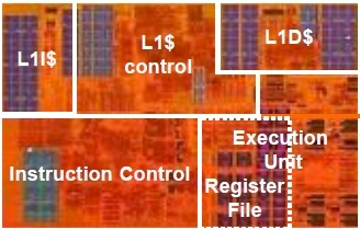
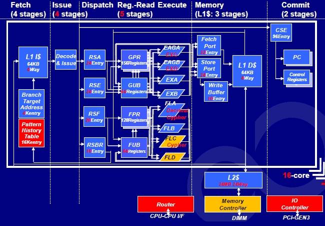
The Sparc64-X core has a deeper pipeline, which enables a higher clock frequency on the processor compared to the Sparc64-VII+, a better branch prediction scheme, bigger queues and floating point registers, more aggressive out-of-order execution, a two-port, multi-banked L1 cache (with twice the bus size and more L1 cache throughput), and a richer set of execution units.
There are two integer execution units, another two virtual address adders that can do double duty as execution units, and four floating point units that can do math and graphics functions. This is twice the number of the integer and floating point units that the Sparc64-VII+ chip had.

The pipeline of the Sparc64-X bears a strong resemblance to the Sparc64-VII+
The Sparc64-X pipeline also adds in a 16KB pattern history table to the branch target address unit that feeds into the L1 instruction cache, which stands pat at 64KB in size. However, that L1 instruction cache, just like the L1 data cache, has been tweaked to be four-way associative, up from two-way with the Sparc64-VII+ chip. The Sparc64-X chip supports two threads per core using Fujitsu's implementation of simultaneous multithreading, just as did the earlier Sparc64 chips.
The die also has one accelerator for decimal math (like IBM has added to its Power and mainframe processors) and two accelerators for doing AES encryption and decryption. These accelerators are parked inside of the floating point units and use their registers.
The new Fujitsu server chip also sports error correction on the registers in the floating point units, adding to the scrubbing on the L1 and L2 caches and parity checking on the integer units. Like the Sparc64-VII+, the Sparc64-X hardware instruction retry, which does exactly what it says it does: re-execute instructions when they get a transient error.

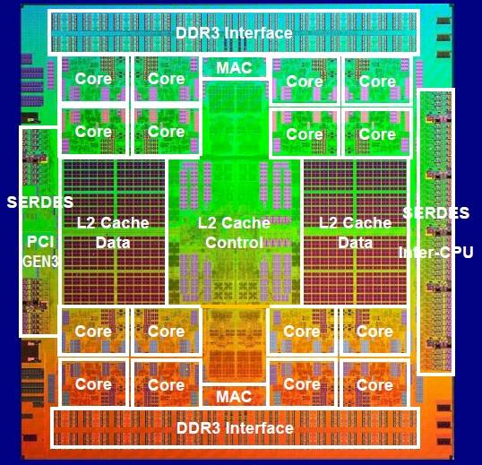
The Sparc64-X die: 16 cores, lots of interconnect, but no L3 cache
The Sparc64-X chip is, like the Sparc64-IXfx for the PrimeHPC supercomputers, a sixteen-core behemoth. It is implemented in Fujitsu's own 28 nanometer processes and packs a total of 2.95 billion transistors onto its die; it is designed to run at 3GHz, which is the same clock speed as the top-end Sparc64-VII+ part.
Given the extra integer and floating point units, the chip should be able to do more work per core. Maruyama said in his presentation at Hot Chips late last week that the Sparc64-X chip could do 288 billion integer instructions per second and 382 gigaflops of floating point math at double precision. The chip has 24MB of shared L2 cache memory, broken into four banks that are situated close to the four banks of cores.
Unlike many modern chips, the Sparc64-X does not include L3 cache, either on the chip, in the package, or on the system board somewhere. This is unusual, but the on-chip interconnect could make up for it. We'll see when Fujitsu runs real-world benchmarks against other machines that do include L3 caches.
The chip has two DDR3 main memory controllers on the die, which delivers a maximum of 102GB/sec of memory bandwidth. The chip also has an on-chip PCI-Express 3.0 controller which has two x8 ports.
There is also a Serdes high-speed transceiver/receiver that implements the NUMA interconnect for the processors that is also on the die. This interconnect has five ports in total for linking sockets to each other, and each port has eight bi-directional lanes running at 14.5Gb/sec. The peak total throughput across this interconnect is 88.5GB/sec, which is twice the bandwidth across the system bus interconnect used with the Sparc64-VII+ servers.

The Sparc64-X interconnect is much simpler than older designs
That interconnect, which is sorely in need of a code-name, allows for four sockets to be gluelessly connected to each other in a NUMA cluster and provides direct links from the sockets to main memory. This is a big improvement compared to the four-way chipset used in prior Sparc Enterprise M machines, which needed two hops to move from processor to processor and which had multiple off-chip circuits controlling access to DDR2 main memory.
The Sparc64-X chip enables a much cleaner server design, and as it turns out a lot more memory bandwidth. On the Stream Triad memory bandwidth test, the old Sparc Enterprise M4000 could do 4.35GB/sec across the DIMM interfaces, but a four-socket machine sporting the Sparc64-X processors was able to drive65.6GB/sec running Stream Triad; that box has four times the cores but fifteen times the sustained, real-world memory bandwidth.
On early benchmark tests, the Sparc64-X chip running at 3GHz was pegged against a Sparc64-VII+ running at 2.86GHz. On a single thread, the new chip delivers about 50 per cent more performance on integer and floating point workloads, which stands to reason given the doubling up of integer and floating point units inside each core.
On 256-bit AES encryption, thanks to those two software-on-a-chip accelerators the performance encrypting and decrypting on the AES algorithm is 14 times faster than on the Sparc64-VII+ processor core. Now, if you want to measure throughput across all of the cores in a socket, then integer, floating point, and Java workloads have about seven times the oomph with the Sparc64-X, and AES encryption is 98 times faster.
Fujitsu is not talking about when the Sparc64-X will come to market in systems, and it was not willing to talk about how much energy this behemoth burns. "But to be frank, this chip is very hot, which is why we are here at Hot Chips," joked Maruyama. A perfectly cromulent answer. ®
