This article is more than 1 year old
Oracle hurls Sparc T5 gladiators into big-iron arena
At my interrupt signal, unleash hell
Hot Chips Oracle's Sparc processor server biz may be bleeding revenue, but the company is still working on very innovative chips. Its Sparc T series, and the Sparc T5 systems that will launch later this year (very likely at the OpenWorld trade show at the end of September) suggest the company is growing its multithreaded processors in terms of cores and sockets and pushing up into the big iron space.
The last time Oracle beefed up its silicon to take on the world's computing beasts, it introduced the UltraSparc-IV+ as a stop-gap to tide customers over until its Sparc subsidiary Sun Microsystems moved the high-end of its product line over to rebadged Sparc64 systems brought in from Solaris partner Fujitsu.
Those dual-core Panther chips came out in 2005 and were enhanced in 2007 ahead of the launch of the Sparc Enterprise M systems from Fujitsu. (And right after Sun had given up on the Millennium UltraSparc-V chips and killed them off.)
Given the scalability enhancements coming from the Sparc T5 machines, which sport faster cores that can do single-threaded work better, they will be big enough for all but the absolutely largest Solaris workloads.
That's not to say that Oracle will drop its reselling agreement with Fujitsu any time soon. There's no indication of that out of Oracle or Fujitsu. Then again, there is also no indication from either Oracle or Fujitsu that the Japanese server maker will be reselling future Sparc T5 machines or that the American server maker will be reselling future Sparc64 X machines. The Oracle and Fujitsu engineers who gave presentations at the Hot Chips conference last week in Cupertino, California did not tell El Reg kept schtum when asked.
The Sparc T5 chip is more than just a shrunken Sparc T4 processor, which Oracle revealed at last year's Hot Chips conference and then started shipping in systems as 2011 wound down. The Sparc T4s had eight of the new S3 generation of Sparc cores, and the 3GHz clock speed and tweaks to the instruction pipeline were designed to make it much better at single-threaded work than its Sparc T chip predecessors. The Sparc T4 is manufactured by Taiwan Semiconductor Manufacturing Corp using its 40 nanometer processes, and the sixteen-core Sparc T5 chip uses the popular 28 nanometer processes from TSMC that a number of processor and graphics card makers are employing in their latest devices.

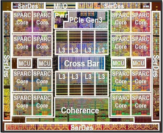
Die shot of the Sparc T5 processor from Oracle
Oracle is using the shrink to 28 nanometer processes in a number of ways. First, it is cramming sixteen cores on the die, double that of Sparc T4 processor. The Sparc T3 chip, based on the S3 core that was pretty terrible at single-threaded work given its design and low clock speed, had sixteen cores as well. But for a lot of workloads, it didn't matter much. For many workloads, such as database, Java, or web serving, the earlier Sparc T2 and T3 processors showed remarkably good performance. With the Sparc T4 chips, Oracle cut back to eight S3 cores and delivered roughly the same performance on OLTP-style work as a 16-core Sparc T3 chip with sixteen cores running at half the clock speed; this makes sense. But the radically redesigned S3 core also provided five times the integer performance and seven times the floating point performance of the Sparc T3s, making the Sparc T4s a more well-rounded and therefore more useful processor for servers.
Getting back to sixteen cores on the Sparc T5 die, each with eight threads for running heavily threaded work, is a good use of the process shrink. Oracle could have gone a simpler route and double-stuffed the sockets with slightly modified Sparc T4 designs, akin to what IBM is doing with its Power7+ processors in some server configurations, to get to that sixteen core level. But, for whatever reason, Oracle wants to have all of the cores on the same die and running on the same crossbar interconnect.
And to help out those monolithic pieces of code that still lurk out there in the Solaris base, Oracle is also using some of the shrink to crank up the clock speed on the S3 cores inside the Sparc T5 chip, in this case up to a maximum of 3.6GHz. The Sparc T4 chips ran at between 2.85GHz and 3GHz.
The S3 core has a 16-stage integer pipeline in both the Sparc T4 and T5 variants, and it has an out-of order execution on its dual-issue pipeline. The threads are dynamically assigned, so if you are running a monolithic piece of code, you can drop back to a single thread per core and let that thread have all of the assets on the chip at its disposal. This is what has radically improved single-threaded performance on both the Sparc T4 and now the Sparc T5 processors compared to their predecessors. The S3 core also supports on-die accelerators for RSA, DH, DSA, ECC, AES, DES, 3DES, Camellia, and Kasumi encryption and accelerators for the CRC32c, MD5, SHA-1, SHA-224, SHA-256, SHA-384, and SHA-512 message digest and hashing functions. The chip also sports a random number generator, which IBM just added with its Power7+ chip.
Sparc T5 chip has 8MB of shared L3 cache, twice that of the Sparc T4 and reasonable given that there are twice as many cores on the die. The Sparc T5 has the same 16KB L1 instruction and 16KB L1 data caches, and also sports the same 128KB of L2 cache on each core as the Sparc T4. The L2 cache could have been boosted, but it seems unnecessary given that the clock speeds of the T4 and T5 processors are pretty close.
Two big differences between the Sparc T4 and T5 chips are on-chip I/O processing and the level of glueless NUMA scaling (meaning without the requirement of an outboard chipset and adjunct circuitry).
The Sparc T4 chip has two PCI-Express 2.0 x8 interfaces and two 10GE interfaces on the die, and it could connect two or four processor sockets lashed together gluelessly into a single system image. With the Sparc T5, Oracle has booted the two 10GE interfaces (or four, if you were thinking there might be four for balance across the cores) from the design and has shifted to PCI-Express 3.0 for the two on-chip x8 peripheral controllers. Ditching the on-chip networking means Oracle could put in circuits for scaling up to eight-socket glueless NUMA clustering, and this is no doubt a good tradeoff.
"There are eight-socket machines on the market that you can buy that only offer the performance of five sockets," explained Sebastian Turullols, hardware director at Oracle's microelectronics unit, in the Sparc T5 presentation. "Maybe they are optimized for four socket performance, but we wanted to deliver linear scaling to eight sockets."

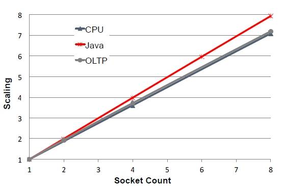
NUMA scaling of the Sparc T5-8 system is nearly perfectly linear
As you can see from the benchmark tests above, Java workloads running across 2, 4, and 8 sockets show nearly perfectly linear scaling. And integer and OLTP work, which has a heavier integer component than Java, both show pretty good scaling as sockets are added to the system. Turullols said that on the OLTP workloads tested, OLTP scaling across eight nodes was as 7.5, which was pretty good considering that on any given node doing work, about 65 percent of the data it needs to process has to come from another node in the system. (The chart above seems to show around 7.25 scaling on OLTP for eight sockets.)
This very good NUMA scaling is done by using a directory-based coherency protocol, Turullols explained, that keeps track of all of the L3 caches in the system and stripes the L3 cache directories across all of the nodes. This approach offers 50 per cent higher effective bandwidth than an implementation that would do a snoop of all the caches in the event of an L3 cache miss.
Within the Sparc T5 chip, cores and caches are linked together by an 8x9 crossbar switch, which sports interleaved address banks, an I/O bridge, independent control and data networks for the L2 and L3 cache on each die that work to warn when data is missing from the caches and to fill them with it when they find that condition. This crossbar has a bisection bandwidth of 1TB/sec, which is twice that of the on-chip crossbar in the Sparc T4 chip. (That is Byte, not bit.) The L2 and L3 caches have a lot of tweaks, many of which are designed to make the scaling across sockets almost as good as the scaling within a socket.

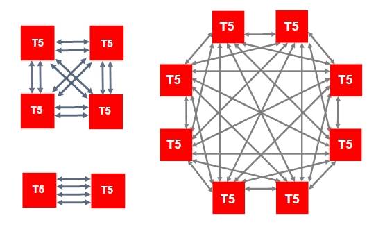
The topology for the cache coherency interconnect for Sparc T5 systems
The on-chip NUMA interconnect in the Sparc T5 systems can offer four links between two sockets in a system, with each link providing 14 interconnect fabric lanes running at 15Gb/sec each. The interconnect supports single-lane failovers if there is traffic contention, and depending on the bandwidth needs in a NUMA system, these inter-socket links can be mothballed on the fly to save energy and fired back up nearly instantly when needed as workloads change. In a four-socket box, there are two links connecting each socket to every other socket in the system, and on an eight-socket machine, Turullols said you need one hop between sockets to scale. It usually takes two hops to get to eight-way NUMA given current designs, so this is where that near linear scalability is coming from. That interconnect can do speculative memory reads, cache-to-cache line transfers between nodes, and dynamic congestion to smooth out the NUMA, too.
The Sparc T5-8 system has over 1TB/sec of memory bandwidth using 1.07GHz DDR3 memory, 840GB/sec of bisection bandwidth across the coherency interconnect that links the processor sockets together, and 256G/sec of aggregate bandwidth across the sixteen x8 PCI-Express 3.0 controllers on the chips.
Much of this stuff was very likely invented for the "Rock" UltraSparc-RK processor that was killed off just as Oracle was in the process of devouring Sun back in the summer of 2009. These Rock chips were supposed to end up in "Supernova" servers that El Reg suspects would look very much like the forthcoming Sparc T5 machines. ®
