This article is more than 1 year old
HGST: Nano-tech will double hard disk capacity in 10 years
Self-assembling molecules to boost drive density
HGST, the Western Digital subsidiary formerly known as Hitachi Global Storage Technologies, says it has developed a method of manufacturing hard-disk platters using nanotechnology that could double the density of today's hard drives.
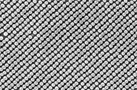
The new technique employs a combination of self-assembling molecules and nanoimprinting, technologies previously associated with semiconductor manufacturing, to assemble patterns of tiny magnetic "islands," each no more than 10 nanometers wide – the width of about 50 atoms.
The resulting patterns are composed of 1.2 trillion dots per square inch, where each dot can store a single bit of information. That's roughly twice the density of today's hard-disk media, and HGST researchers say they are just scratching the surface of what can be achieved.
"With the proper chemistry and surface preparations, we believe this work is extendible to ever-smaller dimensions," HGST fellow Tom Albrecht said in a statement.
The aforementioned self-assembling molecules are so called because they are built from segments of hybrid polymers that repel each other. When coated onto a specially prepared surface as a thin film, the segments line up into perfect rows, like magic.
Once so arranged, the tiny building blocks can be manipulated using other chip-industry processes to form the desired structures before being nanoimprinted onto the disk substrate.

Each of these nano-scale dots can store one bit of data in a space no larger than 50 atoms across (source: HGST)
HGST's key breakthrough was in assembling these otherwise-rectangular features into the radial and circular patterns necessary for spinning-disk storage, which the company says it achieved through careful preparation of the surface onto which the self-assembling molecules were applied.
The chip industry has long eyed nanolithography as a potential alternative to current photolithography processes, which have grown increasingly complex and expensive as the scale of semiconductor features has shrunk.
While it may one day be possible to assemble such complex components as microprocessors using this type of nanolithography, many researchers believe its more immediate use will be for applications such as disk drives or memory, which are simpler and more tolerant of the defects that inevitably occur when employing such an immature technology.
In fact, given HGST's innovations, the first commercial hard drives based on nanolithography may be just a few years away. According to HGST vice president Currie Munce, the company expects the technology to become cost-effective by the end of the decade. ®
