This article is more than 1 year old
Nvidia to stack up DRAM on future 'Volta' GPUs
Over 1TB/sec of memory bandwidth can definitely play Crysis
GTC 2013 Nvidia wants to own an ever-increasing part of the computing racket and will be adding 3D memory stacking to its future graphics processors to make them more power-efficient and to boost their performance.
Jen-Hsun Huang, co-founder and CEO at Nvidia, outlined the company's plans to used stacked DRAM on future graphics chips during his opening keynote at the GPU Technology Conference in San Jose on Tuesday. As he sometimes does, and unexpectedly to his public relations team, Huang whipped out a product roadmap that pushed the GPUs out one more exit on the highway to GPU computing.
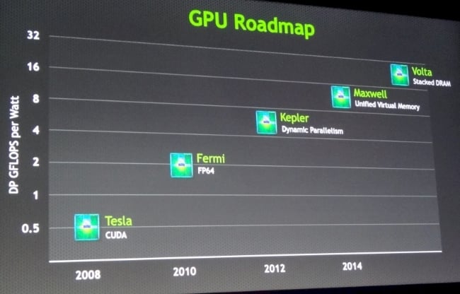
Nvidia is pushing up the performance curve with its Maxwell and Volta GPU chips
The future Volta GPU is named after Alessandro Volta, the Italian physicist who invented the battery two centuries ago. "I love that name Volta because it would suggest that it will be even more energy efficient," explained Huang.
Huang cleverly did not put a launch date on the Volta GPU, but if it is drawn to scale, then we should see it around 2016 or so. Huang did not provide a lot of detail on the future GPU chip, but did toss out a few tidbits to the assembled multitudes in San Jose and those watching from the web.
A number of different vendors are working on 3D stacked memory, with Micron Technology, Intel, and IBM partnering on one effort to stack up DRAM for commercialization in the next few years and a bunch of other efforts underway to try to figure out how to stack up CPUs and memory.
"Volta is going to solve one of the biggest issues with GPUs today, which is access to memory bandwidth," explained Huang. "The memory bandwidth on a GPU is already several times that of a CPU, but we never seem to have enough."
So with Volta, Nvidia is going to get the memory closer to the GPU so signals do not have to come out of the GPU, onto a circuit board, and into the GDDR memory. This current approach takes more power (you have to pump up the signal to make it travel over the board), introduces latencies, decreases bandwidth.
GDDR graphics memory currently wraps around the "Kepler" line of GPUs like so:
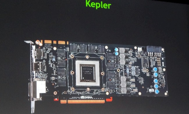
The layout of the Kepler GPU card wraps the memory around the GPU socket
Here is what the layout of the future Volta GPU chip looked like in Huang's presentation:
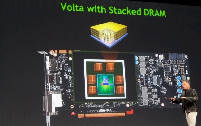
Nvidia is stacking DRAM next to the GPU with its future Volta graphics chip
It doesn't look like Nvidia is going all the way and stacking memory chips and wiring them up directly on top of the future GPU processor. Rather, Huang said that Nvidia will be putting the stacked DRAM and the GPUs onto the same silicon substrate and inside of the same packaging before it welds that package to a peripheral card.
He said the arrangement would look something like what was in the image above, and roughly to scale, which should mean six stacked DRAM units plus a GPU in a chip package sharing a substrate. Huang said that the future Volta GPUs would have an aggregate of 1TB/sec (that's bytes, not bits) of bandwidth into and out of the stacked DRAM, and added that this would be enough to pump an entire Blu-Ray DVD through the memory in 1/50th of a second.
It is not clear what other innovations will be in the future Volta GPU chips, but there will no doubt be many improvements with the CUDA cores as has been the case with the "Tesla," "Fermi," and Kepler generations of GPU chips.
The Tesla chips were glorified GPU graphics chips with the CUDA programming environment added and visualization taken away; the Fermi chips added 64-bit floating point processing to the CUDA cores and as well as error scrubbing on the GDDR memory.
The future "Maxwell" GPU, which looks like it will come out around late 2013 or early 2014 if this roadmap is to scale, has its own memory enhancement, which is called unified virtual memory. Simply put, unified virtual memory will let the CPU to which a GPU is attached see into and address the GDDR memory on the GPU card and conversely will allow for the GPU to see into the DDR main memory that is attached to the CPU in a system.
"All memory will be accessible to all processors, and it will make it a lot easier for you to program," said Huang. "We are trying to improve the efficiency and the performance with each generation, and we are also trying to improve its programability."
With the Kepler GPU chips launched last year, this was certainly true, with the Kepler design being much more energy efficient than its Fermi predecessor. As El Reg explained in detail last year, the dynamic parallelism and Hyper-Q features of the Kepler design allow for the GPU to set its own granularity on a simulation based on the density of data in any particular region in the simulation and also schedule more of its own work rather than bopping back and forth between the CPU and the GPU to get its crunching orders.
GPU computing continues to grow
While gamers and end users working from high-end workstations are going to appreciate the better memory handling and increased memory bandwidth of the Maxwell and Volta GPUs, the biggest beneficiaries might turn out to be those companies setting up ceepie-geepie hybrid clusters, those using number-crunching capacity rented from clouds, or those who use applications that are making use of GPUs behind the scenes to speed up calculations or data sorting and indexing. (Nvidia outlined a bunch of big data uses of ceepie-geepie systems ahead of the GPU Technology Conference and again during Huang's keynote.)
Huang rattled off a bunch of statistics that show how the CUDA environment has grown and the use of hybrid CPU-GPU machines is starting to pick up steam in high performance computing:
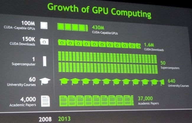
GPU computing has really taken off in the past five years
As part of today's festivities at GTC 2013, Nvidia announced that the Cray XC30 supercomputer being installed at the Swiss National Supercomputing Centre (CSCS) in Lugano, which El Reg told you about last fall, is going to have in excess of 1 petaflops of performance and will be using top-end Kepler K20X GPU coprocessors to do the weather modeling.
Based on information we had last September, the Piz Daint machine was going to weigh in at around 750 teraflops and would not have either Nvidia Kepler or Intel Xeon Phi coprocessors to boost the performance of the Xeon E5 processors at the heart of the machine. But it looks like that has changed.
What El Reg can tell you for sure is that the Swiss Alps region has a lot of microclimates, and doing weather simulations for those microclimates requires some serious horsepower. Nvidia tells us that some of the routines used in the COSMO weather modeling system at CSCS will see a factor of 3X speedup thanks to the additional of GPU coprocessors, and that extra oomph will allow faster and finer-grained calculations to be made for weather prediction.
Piz Daint is expected to be operational in early 2014. ®
