This article is more than 1 year old
Eye spy future HP Moonshot server nodes
Many processors will be coming in small packages for 'Gemini' chassis
Pics HP was at the International Super Computing 2013 conference in Leipzig, Germany, last week, showing off its ProLiant rack servers as well as the SL6500 Scalable Systems tray servers that have been used to build some of the most powerful supercomputers in the world. And, with no tongue in cheek at all, HP's server geeks were also proudly showing off the "Gemini" Moonshot 1500 chassis, and gave El Reg a sneak peek at some future server nodes for its high-density server chassis.
HP is pinning a lot of its server-recovery hopes on the Moonshot 1500 enclosure, and is working hard to get a wide variety of processors and coprocessors fitted for the box, allowing not only for customer choice but also for the staging of workflows across n-tier applications within a single enclosure, with all of the nodes talking across the integrated midplane.
In some cases, these customers could turn out to be traditional HPC users, running simulations across the many processors you can cram into a rack, or the new kinds of HPC workloads, like big data munching.
The Moonshot 1500 chassis launched in early April with a single server node, which was based on Intel's two-core "Centerton" Atom S1200 processor. This was not exactly a speed demon of a chip, and the impending eight-core "Avoton" Atom S1200 v2 chip with its integrated Ethernet ports on the die looks to be a much more interesting proposition for the Moonshot chassis.
The original Centerton server cartridge for had one processor socket and a cutaway motherboard that allowed for a single 2.5-inch disk drive to be snapped right in. And it looks like the impending Avoton card will have the same layout.
Here is the front of the Avoton card:
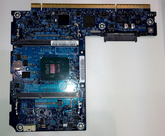
Front view of the future Avoton Atom server cartridge mobo
And here is the view of the back:
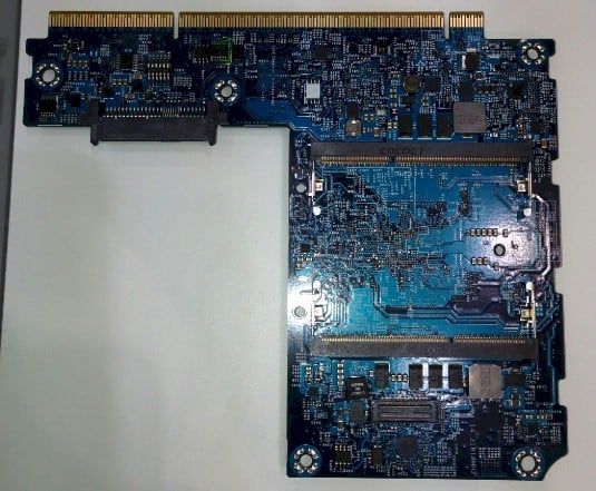
The flip side of the Avoton Atom server board for the Moonshot chassis
As you can see, there is one Avoton processor socket and two memory slots, plus a connector to slide in a single 2.5-inch SATA disk drive. It looks like there are four memory slots for the processor, two on the front and two on the back. So that would be 64GB of memory using 16GB memory sticks.
It didn't have to be this way, by the way. HP also had on hand a four-node Centerton Atom card with an integrated NIC for the four nodes that the HPers said was now defunct with the Avoton card coming out. This four-node Centerton Moonshot cartridge looked a lot like the four-node cartridge that AMD was showing off a few weeks ago in the wake of the debut of its four-core "Kyoto" Opteron X processors.
With AMD getting four sockets and sixteen cores on a cartridge, Intel cannot sit still. At the Moonshot launch, HP said it would work with Intel to get a four-socket Avoton card out, but this card was not at the show. But it will probably look a lot like the quad-node Centerton card that HP said was obsolete already.
ARM processors are getting as much attention as x86 chips with the Moonshot system. A card based on Calxeda's current quad-core ECX-1000 ARM processor, which uses the Cortex-A9 cores, is in the works. The Calxeda ECX-1000 may only be a 32-bit chip, unlike those 64-bit Atoms above, but it has integrated Layer 2 switching on the chip (not a network port, but a switch and network ports) and has enough CPU oomph to be useful for plenty of jobs in the data center where an 8GB memory footprint per server node is sufficient.
Here's the front of the Calxeda Moonshot board, which has four nodes on it:
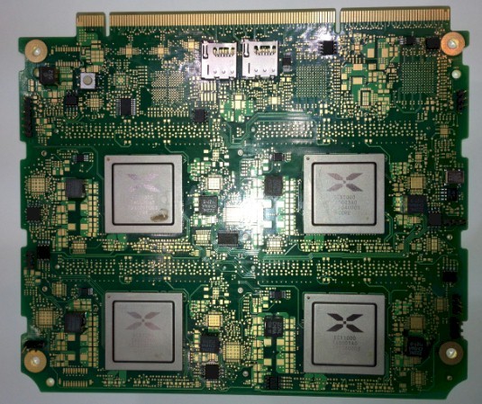
The processor side of the Calxeda card for Moonshot
And here's the backside of the Calxeda card:
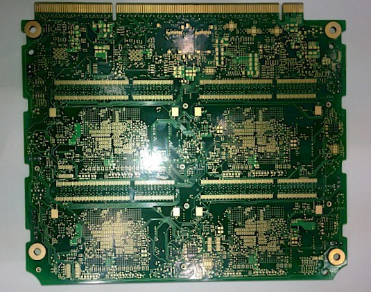
The Calxeda card has one memory slot per socket, just like the EnergyCards that Calxeda made
The memory slots were not yet welded onto this sample, but you can see where they will go. It is not clear how HP will make use of the integrated Fleet Services fabric that is woven across all of the Calxeda chips in a chassis across the backplane, but presumably, if you want to go all-Calxeda, you will not need to use the two integrated Layer 2 switches in the center of the chassis to link the nodes together. You will still need some way to link the Calxeda cards to the outside world, however, and it may be that some of the processing and switch capacity on a Calxeda card can be used to convert it into an uplink for other nodes. No one has been clear how this is going to work yet, and HP is not interested in getting specific until the nodes actually launch, perhaps later this year.
What we can remind you is that the Moonshot backplane has a 2D torus interconnect linking nodes together and can, if need be, ignore the networking on the Calxeda chips. Perhaps for such customers Calxeda will block off that integrated networking and drop prices for those who are just looking for ARM processing and will use HP's networking.
Also sighted at the ISC expo was a future Moonshot cartridge based on the KeyStone-II ARM processor from Texas Instruments, which El Reg caught wind of back in March.
Here's the business side* of the KeyStone-II card:
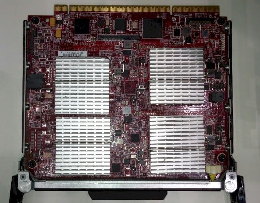
The CPU and DSP side of the KeyStone-II Moonshot cartridge
And here's the party side*:
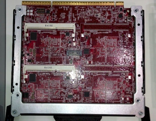
The backside of the TI Moonshot card
There are four of the KeyStone-II chips on this Moonshot cartridge, which are each a hybrid of Cortex-A15 processors with TI's own digital signal processors etched onto the same die. The Cortex-A15 cores have 32-bit processing, but have 40-bit memory addressing (ARM calls this Large Physical Address Extensions). The KeyStone-II chip can have from one to four ARM cores activated, which run at 1.4GHz.
There can be up to eight DSPs on the KeyStone-II chip, delivering around one teraflops of floating point performance at single precision and around 384 gigaflops at double-precision. Throw four of these on a card, and 45 of these in a chassis, and ten enclosures in a rack, and you can cram a lot of computing into a single Moonshot setup. Try 7,200 ARM cores in a rack back-ended by up to 14,400 DSPs with 1.8 petaflops at single precision per rack. I did the math three times on that because it didn't seem possible. If you want double precision, it drops down to 691 teraflops per rack.
The KeyStone-II chips have an integrated switch on the die as well, and a network accelerator that can run at 1Gb/sec and handle 1.5 million packets per second.
As we already explained, with the KeyStone-II design, TI can go after pure cloud infrastructure workloads – servers, switches, routers, network control planes, industrial sensors, and wireless transport devices – with ARM-only versions of the KeyStone II chips. It can activate some of the DSPs on the chip, charge a premium, and go after video, IP camera, traffic system, voice gateway, and medical device applications. And it can turn all eight DSPs on and chase supercomputing, video conferencing, image processing and analytics, medical imaging, and even virtual desktop infrastructure workloads.
It will be interesting to see how these various cards sell against each other. In a way, the Moonshot chassis will be a preview and a proxy for the next wave in the Server Processor War, a wave that will be going on in the data centers of the world for years to come. ®
* Bootnote
Yes, that was an oblique reference to a mullet.
