This article is more than 1 year old
Samsung rolls out first mass-produced 3D NAND flash memory chip
The reports of NAND's death, Sammy says, are greatly exaggerated
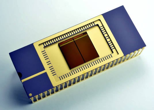
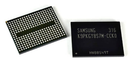
Samsung has announced that it has begun volume production of what it characterizes as "the industry's first" vertically stacked NAND flash-memory chip.
"Following the world's first mass production of 3D Vertical NAND, we will continue to introduce 3D V-NAND products with improved performance and higher density, which will contribute to further growth of the global memory industry," said Samsung SVP for flash product and technology Jeong-Hyuk Choi in a statement.
The V-NAND part will provide 128 gigabits of storage, and is based on Samsung's implementation of 3D Charge Trap Flash (CTF) technology in which, as Samsung explains, "an electric charge is temporarily placed in a holding chamber of the non-conductive layer of flash that is composed of silicon nitride (SiN), instead of using a floating gate to prevent interference between neighboring cells."
CTF has the advantage of being able to be fabricated in higher densities than traditional NAND floating gate structures. According to Samsung, the use of 3D CTF coupled with vertical stacking and vertical-interconnect tech enables their 3D V-NAND to provide more than twice the scaling capability of 20nm planar NAND flash based on floating gates.
Samsung claims that moving the CTF layer into three dimensions not only helps scaling, but also drives up reliability and speed "remarkably," with reliability up two to 10 times and speed that is double that of "conventional 10nm-class" floating gate NAND flash.

A 3D V-NAND presentation package, sporting the colors of the University of California (click to enlarge)
As Choi pointed out, Samsung has big plans for future iterations of the V-NAND tech, including 3D chips with up to 24 layers, all connected by using "special etching technology" to drill down through the layers and connect them electronically.
By doing so, Samsung says, they can achieve greater NAND density without have to further scale down planar tech, a task they call "incredibly difficult to achieve," with the goal of producing terabit V-NAND chips in the foreseeable future.
It would be churlish in the midst of Sammy's moment in the spotlight to point out that newly uncloaked start-up Crossbar announced a one-terabyte chip just yesterday, based not on NAND technology, but instead on resistive RAM, or RRAM – one of the many competitors for NAND's share of the gargantuan flash-memory market.
In a market that size – IHS projects it to be worth $30.8 billion by the end of 2016 – cost-per-chip is going to be what separates the winners from the losers. It's going to be an interesting couple of years, as all of our mobile devices, dense servers, and other applications demand more and more storage capacity.
May the best chip – or chips – win. ®

