This article is more than 1 year old
AMD will fling radical 'Kaveri' chips onto streets in January
CPU and GPU to share memory in heterogeneous harmony
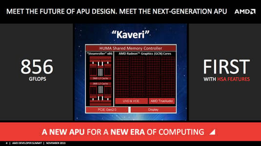
APU13 The desktop version of AMD's next-generation accelerated processing unit, an APU code named "Kaveri", will hit the streets on January 14, the company announced at its developers conference, APU13, in San José, California, on Monday evening.
For those Reg readers not up on AMD terminology, an APU is a mash-up of compute cores, graphics cores, and any other specialized accelerators for video, audio, encryption, or whatever else AMD sees fit to toss on the same die.
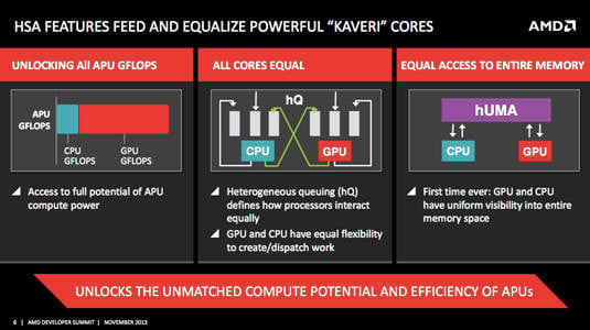
In Kaveri's case, this neologism – neoacronism? – makes perfect sense, seeing as how its compute and graphics cores will share the same system memory in a heterogeneous-computing architecture that AMD dubs hUMA, for "heterogeneous Uniform Memory Access", and which is more generally known as HSA, for heterogeneous system architecture, currently being developed into a standard by the HSA Foundation.
AMD also revealed the performance of the desktop version of the CPU-GPU mashup – a hefty 856 gigaflops – which, thanks to a footnote in AMD's presentation, we learn to be "theoretical GFLOPS calculated by AMD as 856 for AMD A10-7850K with AMD RadeonTM R7 Series Graphics. GFLOPS = CPU GFLOPS + GPU GFLOPS = CPU Core Freq (3.7 Ghz) x Core count (4) x 8 + GPU Core Freq (720MHz) x Radeon Core (512) x 2."
If your eyes glazed over at that footnote, here's the meat: the desktop part for which the performance spec was given will be named the A10-7850K, it will have four CPU cores running at 3.7GHz, and eight GPU cores running at 720MHz each with 512 processing units. The compute cores are based on AMD's "Steamroller architecture.
AMD noted that Kaveri will have "up to 12" heterogeneous compute units – that'll be four compute and eight graphics cores in the part whose performance was cited, but expect different counts in future parts. AMD says that parts for the notebook, embedded, and server markets will appear later in 2014; the desktop parts will fit into an FM2+ socket.
Just how much later those other markets will be addressed by Kaveri, AMD didn't say. They did note, however, that they'll provide more details – including, presumably, pricing and retail availability – at CES in January.
Kaveri is an important milestone for AMD, being the first APU to be based on its "Graphics Core Next" GPU technology, introduced in 2011, the first AMD APU to be fabbed at 28 nanometers, and the first to incorporate the HSA shared-memory architecture mentioned above. It's also the culmination of the 2006 marriage of AMD and graphics powerhouse ATI, with the compute and graphics technologies now sharing not only space on the same die, but also memory.
With AMD having slipped behind Intel in recent years, January 14 will be a big day for fans of Chipzilla's feisty competitor. Intel, however, is already shipping more power-miserly, efficient 22nm chips, and should have it 14nm Broadwell chips ready by next year – and if its new Iris graphics aren't quite AMD Radeon–quality, they're certainly a step up from Intel's previous efforts.
We're crossing our fingers that Kaveri lives up to expectations, and that its HSA/GCN/hUMA goodness finds developers willing to exploit it. Competition is a good thing. ®


