This article is more than 1 year old
Boffins turn nano-wires into their OWN thermometers
Better thermal imaging to help design better electronics
We know that electronic components get hot, but understanding the fine detail of heat in a circuit feature measuring nanometers is difficult.
Infrared imaging relies on wavelengths that are bigger than the features involved, leading to low resolution. Touching a spot with a (tiny) thermometer is high resolution, but its accuracy suffers because some of the heat leaks into the instrument.
US boffins are touting a new approach they say offers high resolution and high accuracy, by using a transmission electron microscope to map changes in density of the device or feature – turning the device, as a University of California Los Angeles (UCLA) canned statement puts it, into its own thermometer.
The technique, called plasmon energy expansion thermometry (PEET), can map temperatures down to a nanometre, the UCLA explains.
In their paper for Science (abstract here), the UCLA and University of Southern California researchers demonstrated their ability to track the heating of a nano-scale aluminium wire heated at one end.
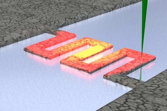
Baby, feel my heat: measuring the temperature of a nanowire is harder than you think
“They focused the microscope’s electron beam to a point, scanned it across the wire and measured the energy of the beam electrons as they came out the other end”, the release states.
Some of the beam's energy is used creating plasmons, and that loss of energy is proportional to the wire's density – and instead of having just one number for the thermal conductivity of the wire, “we get 10,000 numbers as we go down the wire”, says UCLA physicist and astronomer Chris Regan, who led the research with Matthew Mecklenburg, first author of the paper.
Mecklenburg notes that the necessary electron microscopes are already used by silicon-level designers to examine features in their products, so they can use the technique to improve their designs without having to re-tool.
The hope is that if designers can get capture the fine detail of how heat is generated in silicon devices, they can more easily control how heat is generated.
That, in turn, would let them design circuits that either pack more features in the same space, or run at faster clock speeds – both of which are prime sources of increasing heat in integrated circuits. ®
