This article is more than 1 year old
If flash storage achieves FaME, will it live forever?
Introducing your next memory extension
Data access latency has topped the IT sin charts lately and networked flash arrays have been replacing disk drives, doing away with those drives’ rotational delays.
Anything that keeps applications in multi-core virtualised servers running, and not waiting for data while somebody accessing a web commerce page gets impatient and pulls out of an online purchase, is a good thing.
Flash arrays were not fast enough so SSDs directly attached to servers became used for applications that couldn’t wait. But SSDs were not fast enough either, with their SAS or SATA interface, so faster access PCIe flash cards were used instead.
Even PCIe flash cards are not fast enough for some applications and the computer engineer mind has turned to using NAND flash as an extension to DRAM, getting rid of the host operating system's IO code stack and its delay. How would that work?
In the diagram below we have a server – the black rectangle – with DRAM inside in which we find the operating system and any other system software, plus an application and its data.
The application executes and operates inside a memory address space, the server’s RAM allocated to it and which contains its data. When it needs to access this data the app code in effect jumps to a memory address which takes nano/micro seconds.
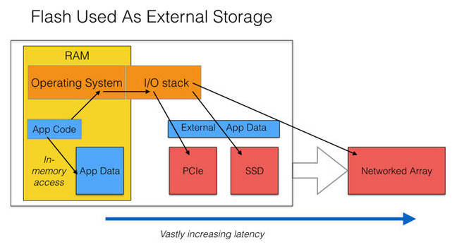
Flash as external storage
However, if the data is not in the internal address space but outside the server’s RAM, then the app requests an IO from the operating system which goes via its IO stack of code and fetches it from a persistent data store. This IO stack traversal – out for the request and back in for the result – occurs for both reads and writes, and it takes time.
The target devices range from PCIe flash cards operating across the PCIe bus accessed in micro-seconds to slightly slower ones such as SSDs connected by SAS or SATA interconnects. A big jump in latency takes us to all-flash networked storage arrays accessed across Ethernet or Fibre Channel, with accesses taking many milliseconds.
We are setting aside clusters of servers with InfiniBand-class inter-connects here for simplicity’s sake, but the same principles apply, with off-server data requests taking longer to fulfill than in-server, in-memory requests.
Any time an app requests data and it is not in the memory address space, then the app code needing the data has to wait, clock tick by clock tick – hundreds of clock ticks, thousands, and even millions of them. In CPU clock tick terms IO waits are extremely wasteful and cause immense delays.
Because servers these days have multiple CPUs, in sockets, with multiple cores which run multiple threads in an app, the cost for an app in lost clock ticks of an IO wait is huge. If a clock tick is worth $1 then a 10 millisecond IO wait costs billions of dollars.
DRAM is expensive and you can’t simply add more and more of the stuff. But suppose you bulk out its address space with cheaper, slower flash and find some way of spoofing the server and its IOS that the flash was DRAM and data stored in it is treated as if it is in the server’s DRAM address space. What then?
The diagram below illustrates this idea:
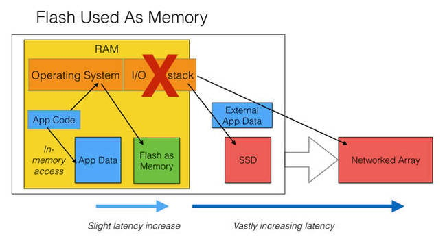
Flash used as logical extension to memory
An app accessing data in this quasi-DRAM flash would not need to treat it as external storage and have its access routed out and back through the operating system's IO stack. That round trip time would simply vanish as the system translates the quasi-DRAM address into an actual NAND address and accesses it in a very short time.
Expanding memory
Fusion-io was an early proponent of the idea of using flash as a memory extension. The concept involved PCIe flash cards being treated as virtual extensions of DRAM at a per-server level. Application data accesses to this virtual memory were affected by PCIe bus and card latency but not by the host operating system’s IO stack latency.
Back in 2012 – yes, that long ago – it used Auto-Commit Memory (ACM) software in a demonstration of eight servers fitted with its ioDrive PCIe flash cards achieving one billion IOPS.
ACM was to be added to its ioMemory Virtual Storage Layer subsystem, the system software controlling access to its ioDrives. It enabled developers to directly control the IO path to the ioDrives so that the host operating system's IO stack could be by-passed.
David Flynn, Fusion's then chairman and CEO, said at the time: "This is not something that could be achieved with hardware alone. Intelligent software that optimises NAND flash as a low-latency, high-capacity, non-volatile memory solution for enterprise servers can transform the way organisations process immense amounts of data.”
Atomic writes were also implemented. These treat writes to multiple independent storage sectors as a single transaction, coalescing them into a single write and speeding up write IOs further.
The ioDrive capacity is seen by applications as an area of memory. Apps simply read or write data from an area of memory, using CPU load store instructions and the ACM API.
This included the directFS API which provided native file-access semantics to flash through a POSIX-compliant file system.
It is implemented directly on ioMemory, significantly reducing latency by bypassing operating system buffer caches, file system and kernel block I/O layers.
Fusion-io directFS is a practical working example of an application running natively on flash to help developers explore the use of Fusion-io APIs.
Steve Wozniak, Fusion-io's then chief scientist, said: “Instead of treating flash like storage, where data passes through all of the OS kernel subsystems that were built and optimised for traditional storage, our core ioMemory technology offers a platform with new programming primitives that can provide system and application developers direct access to non-volatile memory.”
The consequence of this architecture was that application software needed changing to make use of the flash as virtual DRAM. It did not prove that popular and last year SanDisk bought Fusion-io.
Fusion-io's software technology was radical but has since not played a great role in SanDisk’s affairs. Instead the baton has been picked by US startup DSSD, which was acquired by EMC in May 2014.
Promising development
A DSSD all-flash product is expected to be announced this year. We understand it will feature a tightly coupled scale-out design with multi-controller grids, shared memory and transactional commits.
Data access latency should be in the 10s of microseconds through DSSD’s use of in-memory controller technology with its software stack in server memory.
The hardware will be a 5U rackmount enclosure with 36 hot-swappable flash cards, each loaded up with 512 flash dies and a card controller. This flash box will be connected to accessing server hosts across a PCIe fabric using NVMe.
DSSD’s product could store data as objects in a flat address space, with no filesystem structure. There will be software interfacing this hardware to applications in the host that talks HDFS, key value store semantics and other protocols. An application could issue, for example, HDFS IO requests and the DSSD array could respond directly to them.
In other words the need for application code to be modified to talk to the flash, which is presented as a logical extension of the server’s memory, is removed.
This is supposition, as the product has not yet been announced, but it would seem to remove the obstacle that stalled Fusion-io’s ASM/directFS technology.
Prominent role
The Wikibon consultancy described the DSSD technology thus: “The key value proposition of this native attachment is putting very large amounts of non-volatile storage close to the external compute nodes, being addressed as memory."
Since then consultant David Floyer has produced a report describing Flash as Memory Extension (or FaME) as the dominant architecture for enterprise performance computing.
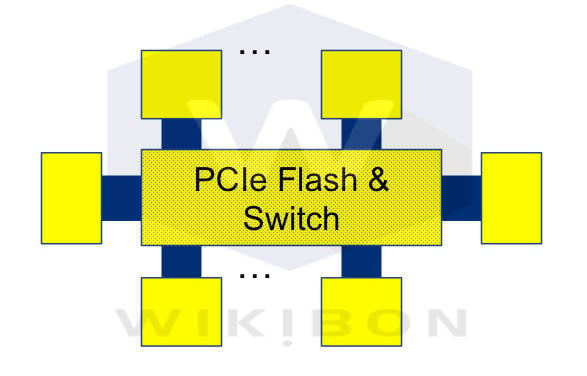
Wikibon consultancy's FaME concept. The yellow blocks are DRAM, the blue block processors and the stippled yellow block the PCIe flash and very low-latency, high-bandwidth switching.
Floyer writes about this diagram: “The logical switch for PCIe flash is a PCIe switch, but other solutions could be viable (flash memory bus DIMMs with memory bus switching may be another alternative). The dotted lines show that there would be many more than six processors. The switch will determine the number of processors within the system, 20-40 processors, being an initial range supported by available technologies.”
He identifies several advantages:
- Applications written and deployed on a two-node architecture will be able to run on FaME with similar performance and can be extended to run with multiple nodes.
- Hadoop applications can take advantage of much faster shared storage and flexible scheduling to reduce significantly elapsed time for completion and minimise tear-down and data loading times for new jobs.
- IO-constrained applications running on an all-flash storage array will complete faster on FaME with lower processor time (reduced CPU wait time).
- Data-in-memory applications can load, reload, recover or restart much faster than traditional configurations because parallel loading and unloading of data can be done 100s of times faster.
This FaME architecture will enable operational transaction systems to co-exist with real-time analytics on the same system. It is extensible “to atomic write APIs within NVMe, which can half the IO required for database applications and double the throughput".
If Floyer is right and the coming DSSD product launch is successful, then we may well see FaME-style server systems being produced by all the server and hyper-converged system vendors over the next 24 months. ®
