This article is more than 1 year old
Intel's Broadwell Xeon E5-2600 v4 chips: So what's in it for you, smartie-pants coders
New instructions, transactions, virtualization features and more
Intel today officially pulls the wraps off its mildly delayed Xeon E5 v4 server processors.
These chips follow up 2014’s Xeon E5 v3 parts, which used a 22nm process size and the Haswell micro-architecture. Intel shrunk Haswell to 14nm, and after some tinkering, codenamed the resulting design Broadwell.
Server and workstation processors using the Broadwell blueprints have been kicking around since early 2015. Now it’s time for the Broadwell-EP Xeon E5 v4s – aimed at scale-out servers – to see the light of day.
Rather than waffle on, we'll keep it snappy for you busy people. Plus, you can check out Timothy Prickett Morgan's take on the Xeon E5s on our sister site The Next Platform, right here.
The Xeon E5-2600 v4 processor overview
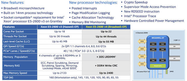
Here’s a summary of the new Xeon E5 v4 chips and how the family compares to its v3 counterparts. Click on any image in this article to enlarge it. The E5-2600 can have up to 22 cores or up to 44 hardware threads per socket, up to 55MB of last-level cache (LLC aka L3), support for up to 2400MHz RAM and DDR4 write CRC. Each core has 2KB of data L1 cache and 32KB of instruction L1 cache, and 256KB of L2 cache.
The extra cores, a smattering of architectural refinements, and the feature size shrink are what gives Broadwell the edge over Haswell.
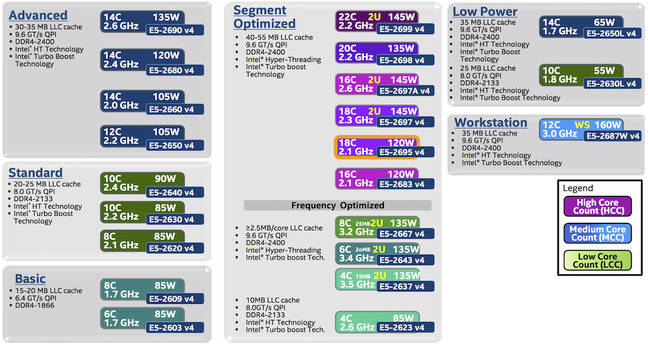
Here’s the two-socket Xeon E5-2600 v4 lineup, where (for example) 14C means 14 cores, along with power consumption and clock speed, which hovers around the 2.4GHz mark. These are what you can expect to order if you’re in the market for a hardware refresh. The Xeon E5 v4 packages are socket compatible with E5 v3 Grantley chips.
OK, that’s the overview – let’s get down to business.
How the cores are arranged
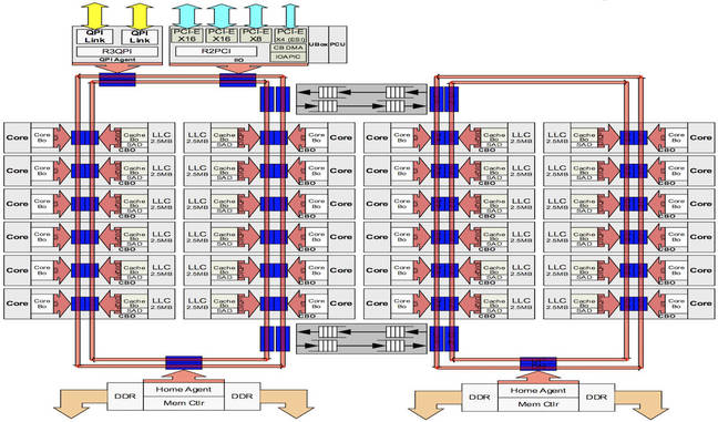
Just as we saw in Haswell, Intel’s Broadwell uses a symmetrical ring-like structure of buses to marry physical CPU cores to caches and the outside world. In a high-core-count chip, say one with 22 cores and 7.2 billion transistors, the processor has two independent rings joined by two interconnects. One ring talks to the QPI and PCIe gen-3 interfaces, and both rings talk to their own RAM controllers that each sport two channels.
The last-level cache is sliced into chunks, and each chunk is plugged into the ring bus structure opposite a core. When a core accesses memory, the requested physical address is hashed and the result used to locate the cache on the ring where the cache line is stored. An L3 cache slice on the ring is not dedicated to the core sitting opposite; instead, the slice could be holding data for various other cores. The hashing algorithm allows Intel to distribute requests for memory over the whole structure. It takes perhaps up to a dozen CPU cycles for a cache request to run the length of a ring to find its cache – we’re told most transactions complete much sooner in a couple of cycles and take the shortest path from the requesting core to the cache holding the data.
Intel’s engineers wouldn’t disclose the algorithm they use so you cannot game the system by engineering your kernel to ensure that cores access just the physical memory that resolves to their nearest cache chunks, thus minimizing the slight latency in running requests around the rings.
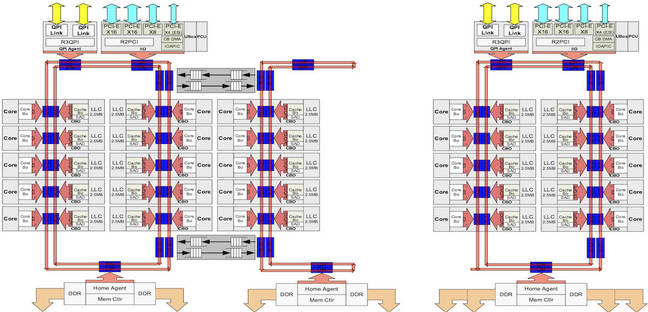
Below, we see a two ring system for high-core-count processors, and Intel’s designs for packages with fewer cores.
Micro-architecture tweaks
Intel reckons Broadwell’s single thread performance is about five per cent higher than Haswell’s in terms of instructions executed per second. It’s achieved this through various tune ups, we’re told.
The vector floating-point multiplication instructions MULPS and MULPD have been reduced in latency to three cycles from five. Similarly, various floating-point division instructions (DIVSS, DIVSD, DIVPS and DIVPD) have been cut in latency. For example, 256-bit single-precision vector divisions have a 16-cycle latency rather than the 20 in Haswell, and double-precision have 22 cycles rather than 34. Scalar divides can be split in two and processed in parallel.
The ADC, CMOV and PCLMULQDQ instructions (the latter being useful in AES encryption) now take just one micro-op, again hurrying along program execution. The translation buffers (TLBs) have been made a little more efficient by increasing the STLB to 1,500 entries from 1,000, and the address prediction for branches and returns has been improved. Broadwell is littered with little adjustments like these to grease the wheels of code execution.
Better use of power when running a mix of math
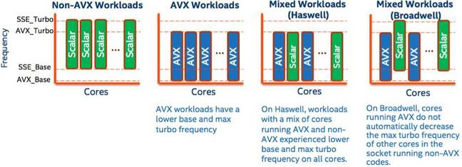
Intel’s vector math crunching instructions AVX tend to make a processor draw more power, so the chip reduces its clock frequency to prevent itself from frying in its socket. Previously, when an Intel processor core started running AVX code, all the cores in the package would be pulled down in frequency. On Broadwell, cores not running AVX code are not slowed down, allowing them to independently run as normal. This means a chip can run a mixed workload of AVX and non-AVX software without paying a penalty.
After a core has not executed any AVX instructions for a set period of time – about a millisecond – it will take the brake off its clock frequency. If your server apps are floating-point math heavy, you may not see much of this power-related feature as you'll be stuck in AVX mode.
Accelerating cryptography
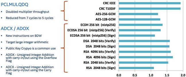
Intel says it’s been able to speed up AES encryption, and ECDSA, RSA and DSA signing and verifying, in Broadwell by reducing PCLMULQDQ from seven cycles to five, and introducing new instructions useful in crypto algorithms. The two new instructions are ADOX (unsigned integer addition with carry-in/out using the overflow flag) and ADCX (unsigned integer addition with carry-in/out using the carry flag). Servers using the new silicon and its additional instructions will have an easier time encrypting, decrypting and verifying your personal data.
The above graphs compare the speed of an eight-core Broadwell Xeon-D with 2x8GB of RAM versus an 18-core Haswell Xeon E5-2699 v3 with 4x32GB of RAM, when running cryptography tests using OpenSSL-1.0.2-beta3 on Linux. For example, the Broadwell Xeon performed the RSA verify operation using a 2048-bit key about x1.5 the speed of its Haswell cousin.
There’s also RDSEED, which is supposed to be used to prime pseudorandom number generators (PRNGs) with random values, which are crucial for strong encryption. If you’re not a massive fan of Intel’s RDRAND instruction due to its black-box design, then RDSEED isn’t going to float your boat either. You can find some technical notes and analysis of RDRAND and RDSEED here and here [PDFs].
Broadwell also brought in Supervisor Mode Access Prevention (SMAP). This lets a kernel set a flag in a control register (CR4) to block kernel-mode code from accessing user-mode memory. This prevents trusted low-level code from unexpectedly tampering – accidentally or maliciously – with applications. A kernel can flip a flag to temporarily disable this check when it really does need to access a process’s address space, such as copying data in and out of an application while servicing a system call.
And, by the way, holy sh*&, Intel’s Transactional Synchronization Extensions (TSX) are back in Broadwell, including the Xeon E5 v4, after the tech was earlier found to be broken.
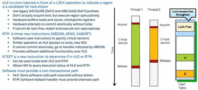
TSX lets programmers mark out the start and end of critical sections of concurrent code, and monitors memory accesses while executing in these regions. Writes and reads to and from memory are redirected to hardware buffers, and at the end of a critical section, data is committed to RAM as expected atomically.
If two threads try to manipulate the same data at the same time in one of these sections, the buffers are discarded, and the threads are rolled back to the start of the critical section. Next, a traditional lock is used to hold one of the threads in place while the other exclusively runs through the critical section.
So if two threads are working on the same data structure, albeit different parts of it and thus do not trample over each other’s memory accesses, there’s no need for a lock at all: the processor treats each thread’s work in the critical section as an atomic transaction. Developers can either use Restricted Transactional Memory (RTM) or Hardware Lock Elision (HLE) to mark out critical sections.
By avoiding the use of locks and using optimistic execution, software can crank through data: databases can processes transactions faster, and apps spend less time spinning needlessly, wasting time and energy. Given its complexity, you can see why it took Intel a couple of goes to get it, we’re told, right.
