This article is more than 1 year old
Microsoft's HoloLens secret sauce: A 28nm customized 24-core DSP engine built by TSMC
How to make your own virtual reality brain
Hot Chips Microsoft today revealed a first look at the inside of its Holographic Processing Unit (HPU) chip used in its virtual reality HoloLens specs.
The secretive HPU is a custom-designed TSMC-fabricated 28nm coprocessor that has 24 Tensilica DSP cores arranged in 12 clusters. It has about 65 million logic gates, 8MB of SRAM, and a layer of 1GB of low-power DDR3 RAM on top, all in a 12mm-by-12mm BGA package. We understand it can perform a trillion calculations a second.
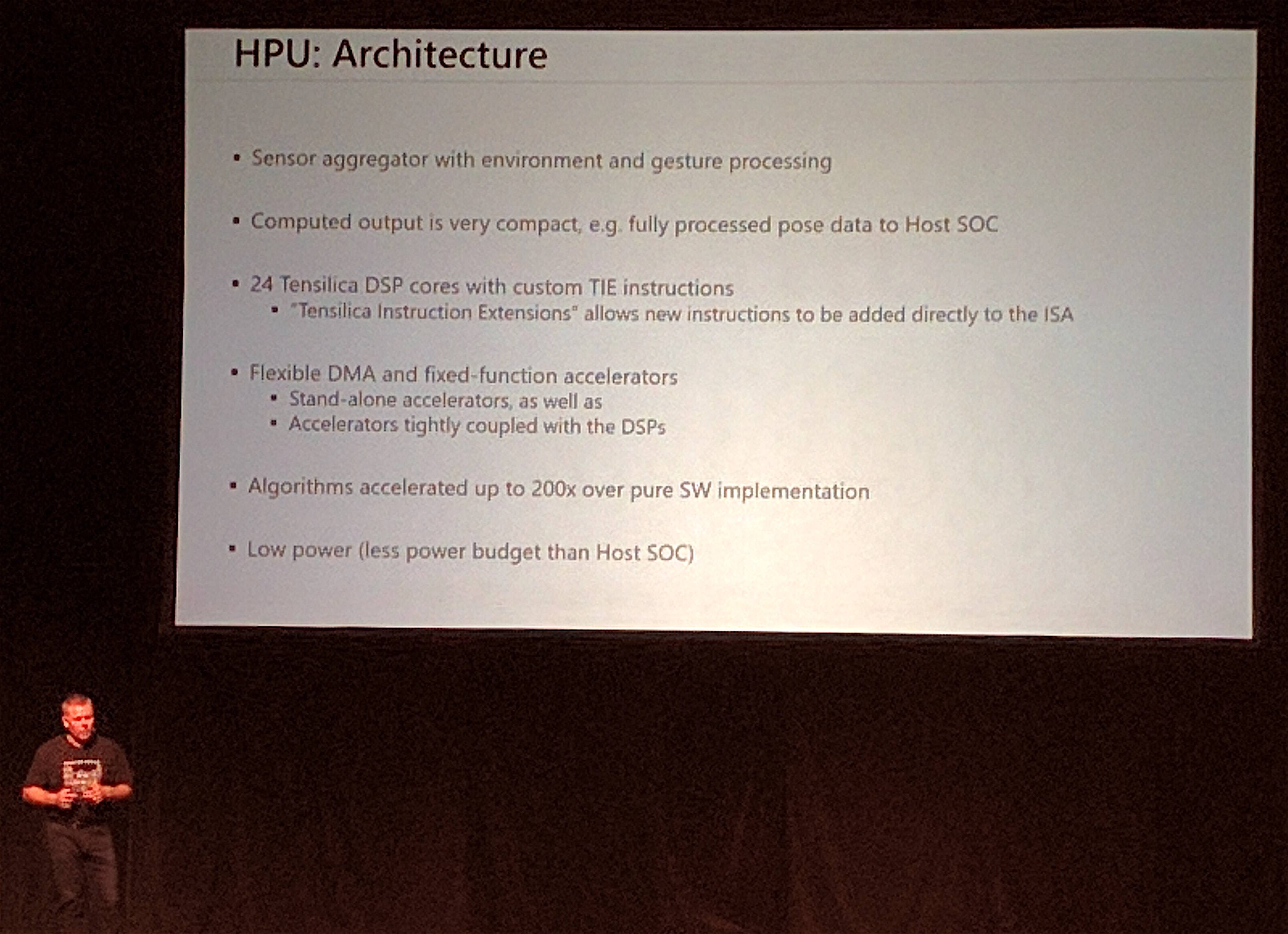
It handles all the environment sensing and other input and output necessary for the virtual-reality goggles. It aggregates data from sensors and processes the wearer's gesture movements, all in hardware so it's faster than the equivalent code running on a general purpose CPU. Each DSP core is given a particular task to focus on.
The unit sits alongside a 14nm Intel Atom x86 Cherry Trail system-on-chip, which has its own 1GB of RAM and runs, in 32-bit mode, a flavor of Windows 10 and apps that take advantage of the immersive noggin-fitted display.
The details were revealed today at the Hot Chips conference in Cupertino, California. We grabbed a snap of the slides – apologies for the blurriness, we were sitting far back to get a decent Wi-Fi signal.
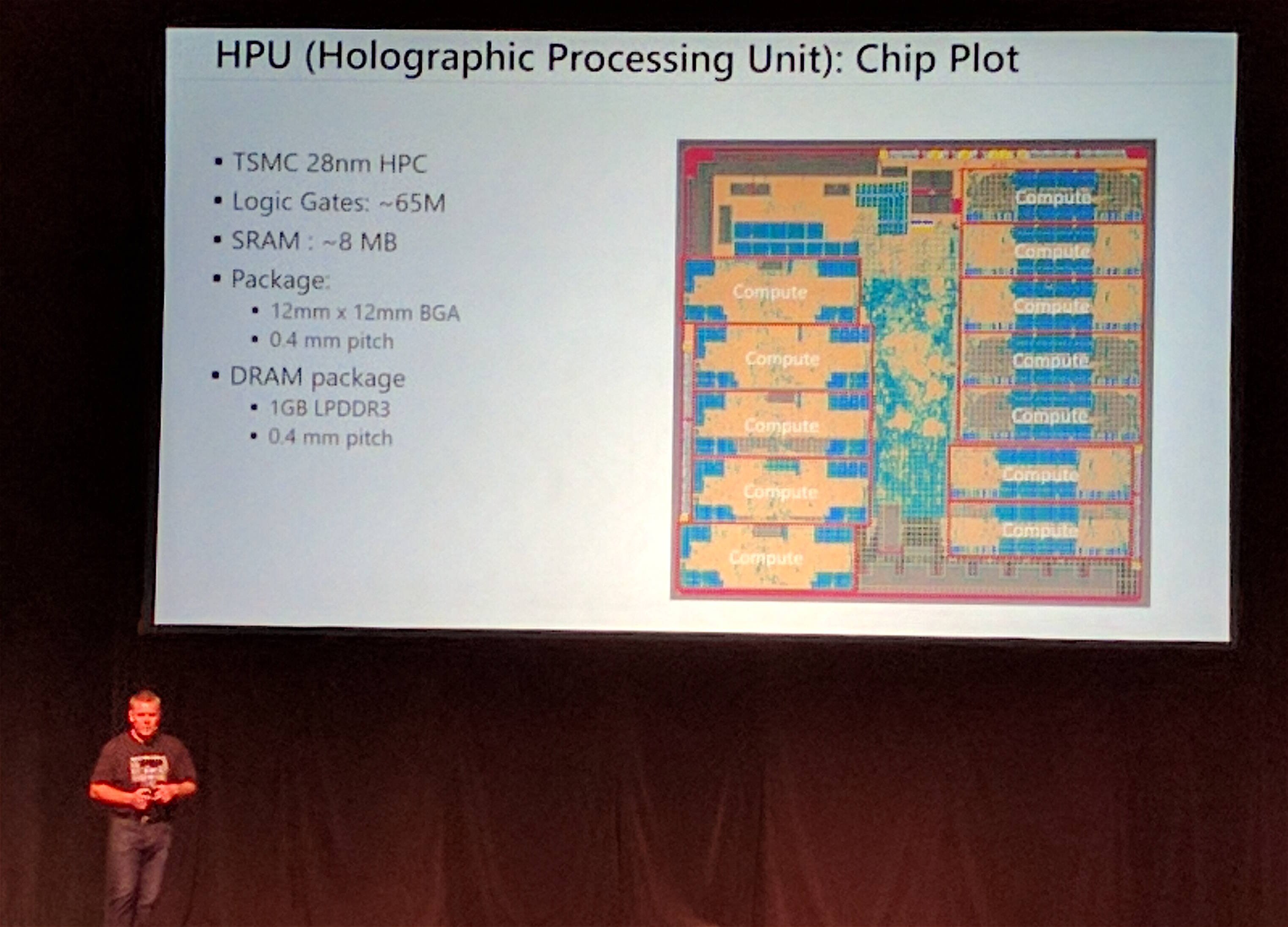
The floor plan of the custom HPU with 24 DSP cores in 12 clusters ... Click to enlarge
The HPU draws less than 10W and includes PCIe and standard serial interfaces. Microsoft took Cadence’s Xtensa base instruction set and added various custom instructions to the DSPs to speed up specific operations needed by the HoloLens to render realtime augmented reality. Overall, the unit is capable of accelerating algorithms to 200 times faster than when in pure software.
Data shuttled over to the host Atom processor is as cooked as possible, meaning the x86 CPU shouldn't have to do lots of extra processing work on the information taken from the HPU.
The main advantages of using the Tensilica designs ... Click to enlarge
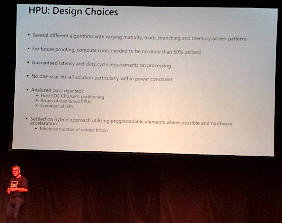
The slides and information were revealed by Microsoft Devices Group engineer Nick Baker, who said Redmond rejected using traditional CPUs or CPU-GPU SoCs in favor of a bespoke design that includes hardware acceleration and programmable elements. None of the DSP cores are each pushed beyond 50 per cent capacity at the moment, thus future-proofing the product. Finally, the HPU's design allows Microsoft's engineers to guarantee latency and duty cycles during processing.
According to Baker, the chip was extensively simulated prior to its initial fabrication, and the first physical prototypes worked first time.
The HoloLens started shipping to developers in March, and next year Windows 10 PCs can use it to provide a 3D desktop environment. ®
