This article is more than 1 year old
Hopping the flash stepping stones to DIMM future
How levels, layers, stacks and DIMMS are boosting speeds
Analysis Up until very recently the main thrust of data access and storage technology development was to make the media faster, hence the move from disk to flash, and flash technology developments to increase capacity.
But the opportunity to make further advances is closing and attention is turning to removing the final obstacle to fast stored data IO, the operating system code stack. Removing that really will enable stored data access to run at memory or near-memory speed and revolutionise stored data IO forever.
The road to there starts here, with the current transition from storing data on disk to storing it on flash, in SSDs. The obvious reasons for this are that flash access latency is sub-millisecond, whereas disk latency can be 20 - 100 milliseconds, that flash takes up less physical space, and that it uses less electricity and needs less cooling.
As its reliability and endurance have risen - and cost has come down, helped initially by deduplication and compression reducing the amount of data that needs to be stored - flash is taking over the duty of storing primary data and beginning to move into secondary data storage.
Flash is a constantly developing storage medium. The initial planar or 2D NAND, involving a single layer of flash cells, stored 1 bit per single level cell. The cell is set by applying a write-level voltage and is read by testing its resistance level with a threshold voltage. If current flows then the applied threshold voltage has beaten the resistance level and indicates a binary 1 in the cell, and if it does not flow then a binary 0 value exists.
The way to get more capacity in a NAND die was to shrink the cell size, using a smaller lithography, to cram more cells into the die. Thus 80nm-type cells gave way to 70nm-type ones, and then 60nm, 50nm and so on down to 14nm after which point there are fewer and fewer electrons left in the cell to produce a reliable signal reading. So cell size shrinkage produced a dead-end that had to be avoided or delayed to further increase capacity and reduce cost.
The answer was twofold, involving levels and then layers.
More levels (bits)
It was possible to add more bit values to a cell by effectively sub-dividing its resistance level range (basically all or none in an SLC cell and hence two states) into four states for a 2bits/cell product. That doubles capacity so a 50GB SSD becomes a 100GB one, produced on the same manufacturing process and so roughly half the cost.
This was called MLC for multi-level cell NAND - before manufacturers realised they could sub-divide further, into eight states and have 3 bits/cell, which is called TLC (Triple-Level Cell) NAND with a 50 per cent capacity increase over MLC. And now manufacturers are wondering about having 4 bits/cell with QLC (Quad-Level Cell) technology and another 25 per cent capacity increase.
Here is how these multiple value cells work, with possible binary values for SLC, MLC, TLC and QLC cells being:
- SLC = 0 or 1 - meaning two states and one threshold voltage,
- MLC = 00, 10, 01, or 11 - four states and so three threshold voltages,
- TLC = 000, 001, 010, 011, 100, 101, 110, 111 - eight states and thus seven threshold voltages,
- QLC = 0000, 0001, 0010, 0011, 0100, 0101, 0110, 0111, 1000, 1001, 1010, 1011, 1100, 1101, 1110, 1111 - 16 states and so 15 threshold voltages.
We can’t go on adding more bits because SSD controller technology can’t cope with the precision and errors involved. Also, each extra cell bit slows SSD speed and shortens its endurance, meaning the SSDs don’t perform as well or as long. Here is where extra layers come in.
More layers
It’s possible, with careful manufacturing, to have more than one layer of cells, and so increase capacity by increasing the vertical height of the flash die. So 24-layers were checked out, and then 48-layers, with Samsung taking the lead, and SanDisk/Toshiba following in its footsteps while Intel and Micron pondered whether it was more cost-efficient to stay with planar NAND for longer.
It was easier to produce 3D NAND with larger cell sizes than the then current 2D NAND, which meant that each cell had more electrons, and thus performed faster and for longer at any bit-level state – SLC, MLC, or TLC. Samsung is now producing 64-layer, TLC 3D NAND (or V-NAND) SSDs, with huge capacities – 7TB and 15.3TB, bigger than 2.5-inch disk drives. Planar TLC NAND is stuck at the 2TB or 3TB level and so now every manufacturer is moving to 3D NAND technology.
They are all looking at the 64-layer level and hoping to go to 96 layers and even further as ways of continuously increasing capacity. But problems loom. Building a multi-layered chip means stacking layers incredibly precisely atop one another and then constructing (etching) holes between the layers for connecting wires. These holes have to be precisely vertical and have a precise diameter and intersect with precisely the right features in each layer as they go down through the chip. It is an extraordinary feat of manufacturing technology. A 0.01 degree per layer error in any direction at the top layer becomes a 0.48 degree error at the bottom of a 96-layer stack and that could mean features are missed and the die is a dud.
Now add another 24 layers and/or shrink the cell lithography and the error tolerance is even less.
We will probably get to 96 layers. Whether we’ll be able to shrink the cell lithography while doing that is a moot point. But, anyway, another technology dead-end seems to be looming capacity-wise and a different technology, a post-NAND technology would be needed to get over that.
Post-NAND media technologies
The most prominent post-NAND technology is Intel and Micron’s 3D XPoint (CrossPoint) which uses a bulk-change mechanism in a chalcogenide glass medium to alter its resistance. This technology is claimed to be both denser than NAND (more capacity in less space) and faster. But the actual mechanism is a secret and XPoint is only just being sampled in Optane SSD form, with faster-access DIMM-mounted XPoint due later this year and close Intel CPU-coupling (Purley CPU and Omni-Point interconnect possibly) in 2018.
Samsung has an intermediate and competing Z-SSD technology which is some secret way of developing NAND to increase access speed to near-DRAM levels. Then there is a WD (SanDisk) resistive RAM technology under development together with an HPE-only variant of ReRAM, the memristor. We also have IBM researchers looking at Phase-Change Memory, and startups focussing on Spin-Transfer Torque RAM (STT-RAM), EverSpin for example.

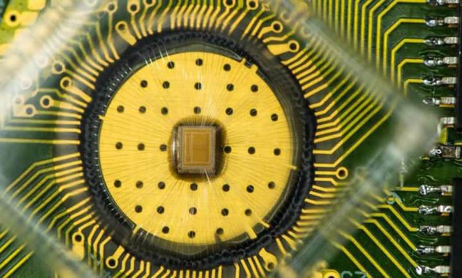
IBM Phase-Change Memory
All these technologies will provide what’s called Storage-Class Memory (SCM), persistent (non-volatile) storage accessed at memory speed. In a computer, memory is accessed directly, being byte-addressable and accessed with, for example, load and store instructions. Traditional storage (not storage-class memory) is accessed via an IO code stack that reads and writes files or blocks of data to a block-access drive full of non-volatile media; paper tape, magnetic drums, rotating disks, magnetic tape and, of course, latterly NAND flash.
In CPU cycle terms traversing the IO stack takes thousands of CPU cycles; it wastes CPU time, it delays application execution but it's necessary because the storage devices are zillions of times slower at doing their thing than CPUs are at doing theirs. So the CPU initiates a context switch for an IO and moves to processing another app, another thread, when one issues an IO.
If storage operates at memory or near-memory speed then the data could be read and written directly from/to the medium and there would be no need for a time-consuming IO stack’s involvement.
Keep this thought in mind as we context switch ourselves and look at non-volatile storage’s access speed. These two threads will ultimately come together.
The need for speed
Meanwhile, just as one part of the industry has focussed on increasing SSD capacity, another part has focussed on increasing its access speed. When SSDs first came in they were built as quasi-disks to fit in disk drive slots in host systems, hence 3.5-inch and 2.5-inch form factors, and SATA and SAS interfaces. Then suppliers figured sticking these fast drives on the PCIe bus meant data access was faster and latency lower, which meant more IOs per second (IOPS). A PCIe card could also have more real estate on which to mount flash chips and so increase capacity.
But each supplier’s PCIe flash card had to have its own driver for every different host system, which was idiocy compared to the standard SAS and SATA drivers available. Quickly the industry realised a standard driver was needed and this is called NVMe (Non-Volatile Memory Express). We’re now seeing a flood of NVMe SSDs hitting the market with more coming.
Are you getting the picture here? The NAND media, device and interconnect areas are in perpetual motion as suppliers try to constantly and simultaneously increase device capacity and get data access speed closer to raw NAND access speed. So SATA and SAS were improved from 3Gbits/secs to 6Gbit/sec and on to today’s 12Gbits/sec while PCIe is faster still, but it is still a hop away from a host system’s CPU-Memory bus, the gold DRAM-speed interconnect standard. NetList and Diablo Technologies have pioneered putting NAND directly on memory DIMMs and so directly connecting to the memory bus.
Software obstacles to faster data access
Although this provides, in theory, the very fastest NAND data access, server manufacturers have been slow to adopt it, because realising that speed requires operating system and application software changes.
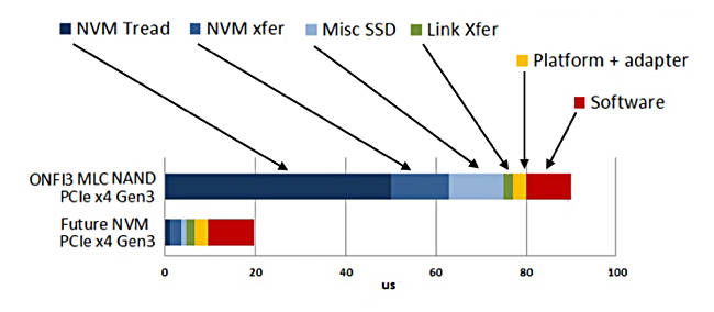
Let’s step back a moment, and consider that continually making the media faster brings in diminishing returns, because there are other elements causing access latency which faster media does not fix. Here is a diagram showing this;

Data access latency contributions from Jim Handy of ObjectiveAnalysis.
The IO stack is becoming the single most important obstacle in the way of increasing data access speed and, now, with SCM it can be sidestepped.
IO stack sidestep
SCM implemented as memory or near-memory speed NVDIMMs can be accessed in a way that delivers partial IO stack latency reduction by having an SCM driver added to the host operating system. It receives file-level IO semantics (read file, write file, etc) from the OS and translates those into memory level (load, store) semantics for the storage medium on the DIMM. Using a DRAM DIMM with non-volatility provided by battery- or capacitor-backed NAND (NVDIMM-N) means this can be about ten times faster than IO stack-level access to an NVMe SSD. This is termed block-level access to the NVDIMM.
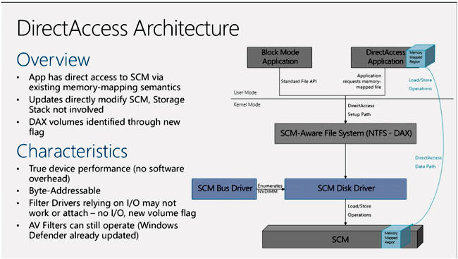
If we use byte-level access to the NVDIMM, by having the OS treat it as a direct-access volume (DAX in Microsoft terminology) so modified application code can issue memory-level load-store commands directly to it then block-level time wasting is avoided and the NVDIMM is accessed eight times faster again, meaning 80 times faster than the NVMe SSD.

Microsoft DAX architecture for Windows Server 2016
These comparative numbers are based on Microsoft tests which revealed:
- In a simple 4K random write test using a single thread against an NVMe SSD the latency was 0.07ms (70 microsecs) and bandwidth about 56MBps,
- Running the same test in a block mode NVDIMM-N we see 0.01ms (10 microsecs) latency and 580MBps, 10 times faster,
- Running the same test in byte-addressable mode the result is eight times faster still, more than 8GBps at c820ns latency.
You can explore the background context to this here.
The benefit to all this is not just that tens of thousands of CPU cycles can be saved per app per unit of time, but that the host system CPUs stop spending 30, 40, 50 or more percent of their time doing IO handling, for which there is now no need, and can do more useful work. Put very crudely it’s as if a 40 per cent recovery of CPU resources in a server means up to 40 per cent more virtual machines can be run, or an up to 40 per cent cheaper server used, as well as having existing VMs run faster.
It is like having layers of OS code friction removed that currently slow everything down.
Takeways
- MLC and TLC 3D NAND SSDs are now the norm for storing primary data
- NVMe access protocols are taking over from SATA and SAS
- Enhanced layering of 3D NAND SSDs will enable flash to cost-effectively start storing secondary data
- DRAM/Flash NVDIMMs will enable IO code stacks to be side-stepped to gain near memory, byte-addressable storage access speed
- 3D XPoint and/or other media will enable NVDIMMs to substitute for DRAM with greatly increased capacities
- Non-volatile SCM DIMMS with direct access volumes will radically increase server (and ultimately client) stored data access speed
All this will be - and is being - achieved by adding layers and levels to NAND, by mounting the media on DIMMS and then getting rid of the IO code stacks. It’s a rosy future and one that is only a few years away. Close your eyes and it will be here in a flash. ®
