This article is more than 1 year old
Wanna design a chip that talks to silly-fast GDDR6? You'll have to talk to Rambus, too
Blueprints touted to ASIC, SoC makers to take on GPUs
Patent troll Semiconductor licensing giant Rambus announced this week a physical layer design for accessing GDDR6 – aka double data rate type six synchronous graphics random-access memory.
This GDDR6 PHY blueprint is aimed at hooking up high-speed, high-bandwidth GDDR6 SGRAM to hardware accelerators and processors to rapidly crunch through stuff like crypto-mining and machine learning.
GDDR technology is usually aimed at plumbing fast memory into graphics processors to make games and math-heavy workloads run faster. These Rambus designs are aimed at non-GPU semiconductor engineers who want to connect super-fast dual-channel GDDR6 SGRAM to their custom accelerators and system-on-chips.
The upshot for non-computer-engineers is that you may see more stuff, other than graphics cards, on the market soon that can plug into nippy GDDR6 SGRAM, using this technology.
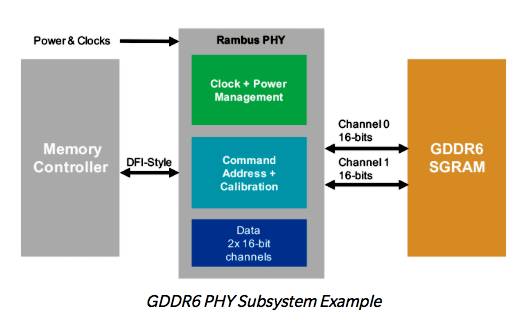
Rambus's tech can talk to GDDR6 storage at up to 16Gbit/s per pin – double the speed of single-channel 8Gbit/s GDDR5. That's five times faster than DDR4 RAM, which has 3.2Gbit/s of bandwidth. Each GDDR6 channel is 16 bits wide, making 32 bits in total for this dual-channel architecture.
The Rambus GDDR6 PHY supports a total maximum bandwidth of 64GB/sec, and is fully compliant with the JEDEC GDDR6 (JESD250) standard. The PHY links the actual memory to a memory controller, and is expected to be embedded in an ASIC or system-on-chip:
Micron, Rambus, and Avery Design are working together to encourage GDDR6 adoption outside the GPU market by providing the following parts and blueprints to chip and system architects:
- GDDR6 memory (Micron 8Gb parts with 16Gb coming)
- GDDR6 PHY design, from Rambus
- GDDR6 controller, from Northwest Logic
- GDDR6 verification IP, from Avery Design
The Northwest Logic GDDR6 controller can be fully integrated, verified, and delivered with the Rambus GDDR6 PHY to help engineers create GDDR6-capable chipsets. GDDR6-based SoC designs can then be verified and performance-optimized using the Avery Design IP.
Silicon products using GDDR6 may appear later this year.
Rambus will demonstrate memory channel signalling at GDDR6 speeds at DesignCon in Santa Clara, California, between January 31 and February 1. ®
