This article is more than 1 year old
Heads up: Fujitsu tips its hand to reveal exascale Arm supercomputer processor – the A64FX
AKA how it learned to stop loving SPARC64
Hot Chips Fujitsu has unfurled the blueprints for its homegrown high-performance Arm-based processors dubbed A64FX, the brains of its Post-K supercomputer.
The designs were shown on Tuesday at a gathering of semiconductor engineers in Silicon Valley. The Post-K is a 1,000 peta-FLOPS monster – an exascale machine – that will supersede Japan's SPARC64-based K supercomputer. It is due to go online in 2021, and has just completed a round of trials that demonstrated the processors work – to some degree, at least.
Post-K hopes to be the world's fastest publicly known supercomputer by the time it's fully powered up and consuming 30 to 40MW. Today, the top slot is held by the US government's Summit machine that uses IBM POWER9 and Nvidia Volta GV100 processors, along with Mellanox networking gear, to max out at 188 peta-FLOPS while consuming 8.8MW.
Crucially, it will be an exascale Arm-compatible supercomputer, a significant milestone for the CPU architecture that's famous for being in practically everyone's phones, hard drives, smart cards, and other embedded electronics, and has dreams of driving laptops and servers.
So what does a Fujitsu-designed supercomputer Arm processor look like? Here's what we learned from Fujitsu's Toshio Yoshida at the Hot Chips engineering conference in Santa Clara: the A64FX has 8.8 billion 7nm FinFET transistors in a package with 594 pins, and 48 CPU cores plus four management cores. Each chip has a total of 32GB of high-bandwidth memory (HBM2), 16 PCIe 3.0 lanes, and a 1024GB/s total memory bandwidth, and hits at least 2.7 tera-FLOPS in terms of performance.
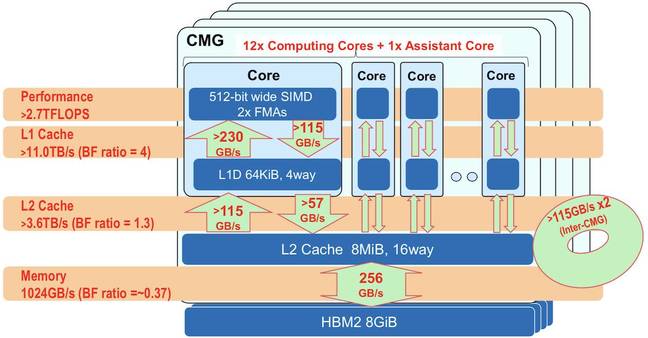
The 52 CPU cores are split into four clusters of 12 main cores plus one management core, each group has 8GB of HBM2 rated at 256GB/s, and 8MB of shared L2 cache. There is cache coherency across the clusters and the whole chip.
The chips are interconnected via Fujitsu's second-generation Tofu mesh-torus-like network. This interconnect can shift data, in and out of each processor chip, via 10 ports each with two lanes maxing out at 28Gbps each.

The A64FX's cache hierarchy and speeds, for the 12 compute cores and management core per cluster, four clusters to a chip ... Source: Fujitsu
Click to enlarge
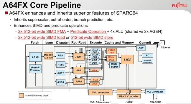
The CPU cores are 64-bit only – there's no 32-bit mode – and they use the Armv8.2-A instruction set. It supports Arm's 512-bit-wide SIMD scalable vector extension (SVE) that we described in detail, here. It means the chips can crunch vector and matrix calculations in hardware – a must for supercomputer and machine-learning applications. It also supports 16 and 8-bit integer math, as well as the usual floating-point precisions (FP16, 32, and 64), which are useful for AI inference code.
The A64FX is a superscalar, out-of-order execution beast, and first Armv8.2-A design, we're told. Folks who have done 32 and 64-bit Arm assembly programming will know the architecture has fixed-width instructions, typically one operation per instruction, as per the classic RISC school of thinking. Interestingly enough, the A64FX, by implementing SVE, has an instruction prefix for its four-operand fused-multiply-add instruction (FMA4) – an incredibly useful operation – that kinda reminds this vulture of x86 instruction prefixes.
To perform the calculation r0 = r3 + r1 * r2, you use two instructions that are merged into one at the pre-decode stage, and are performed in one step despite being fetched as two instructions. These are:
movprfx r0, r3      ; prefix next instruction
fma3 r0, r0, r1, r2 ; r0 = r3 + r1 * r2, the r3 substituted in
Each CPU core's execution unit can handle two 512-bit SIMD operations at once. The input data is packed into 512 bits and crunched in one go – like Intel's AVX512 operations on its server parts. So you could feed in four 8-bit values, four corresponding 8-bit coefficients or weights, which are multiplied to get four answers then added to a 32-bit offset, and written out to a register.
Fujitsu reckons its A64FX can hit 21.6 TOPS (trillion or tera operations per second) when doing 8-bit integer math; 10.8 TOPS with 16-bit integers; 5.4 TOPS with 32-bit; and 2.7 TOPS with 64-bit, all when performing integer SIMD. Overall, it's said the A64FX is at least 2.5 faster than Fujitsu's previous supercomputer processor – the SPARC64 XIfx – at HPC and AI work.
Nvidia's P4 and P40 accelerators for servers clock in at 22 and 47 TOPS with 8-bit integer, for what it's worth.
The L1 cache has a combined gathering mechanism that can fetch consecutive elements in arrays and copy them into a register. So, for example, you could use this to hoover up eight bytes spread over memory into one 64-bit register, each byte slotted into its own byte position in the register. The per-core four-way 64KB L1 data cache is read by the instruction engines at 230GB/s, and written back at 115GB/s. The L2 shared cache feeds data in at 115G/s, and receives at 57GB/s.
Per-chip power usage is monitored and controlled on a per-millisecond basis, and down to the nanosecond per-core. Fujitsu claims its A64FX has mainframe-grade resilience, with ECC or duplication on all caches, parity checks within the execution units, instructions are retried if something is detected as going wrong, error recovery on the Tofu interconnect links, and 128,000 error checkers in total on the chip.
The whole shebang runs Linux, with a Lustre-based distributed file system and non-volatile memory for accelerating file input-output. The toolchain supports C, C++ and Fortran compilers, MPI, OpenMP, debuggers, and other utilities and languages.
You'll note there are no third-party accelerators: it's pure Arm, Fujitsu's way. The aim is to design a chip that runs supercomputer-style applications – simulations, science experiment analysis, machine learning, and other number crunching – with a higher performance-per-watt than general-purpose CPUs.
Yoshida didn't want to talk about clock speeds and individual chip power usage just yet, sadly. The machine is still years away from being finished, and all the specifications and implementation details have yet to be nailed down or revealed. "We will continue to develop Arm processors," he told the conference, though. Despite its delays, Fujitsu hasn't been put off Arm big iron.
And, er, yes, you might be able to play Crysis on it. ®


