This article is more than 1 year old
What the PUC: SK Hynix next to join big boys in 96-layer 3D NAND land
Whether you Periphery Under Cell or Core Over Periphery, it all means smaller chips
SK Hynix has finished work on a 512 Gbit, 96-layer, 3D NAND chip with 1Tbit, and 3bits/cell (TLC) and 4bits/cell (QLC) coming later.
Currently SK Hynix is shipping 72-layer 3D NAND chips. The 96-layer chip uses charge trap flash (CTF) tech, as opposed to floating gate, and its logic circuitry is placed underneath the flash cells. SK Hynix calls this Periphery Under Cell (PUC) tech, and it follows what rivals are doing – all building physically smaller chips as a result.
Micron uses a similar scheme to place peripheral logic at the base of the chip, which it calls CMOS Under the Array (CUA). Samsung is building charge trap flash chips with >90 layers and has also placed the logic underneath the chip, calling it Core Over Periphery (COP).
China's YMTC has put its logic circuitry on top of its chips, but the net effect is the same.
SK Hynix has described its product as CTF-based 4D NAND Flash and said it will start mass-producing 96-layer chips by the end of the year. Its 4D NAND chip has shrunk by more than 30 per cent and increased bit productivity per wafer by 49 per cent compared to its 72-layer 512Gb 3D NAND, the company claimed.
The new chip has a 30 per cent higher write speed and 25 per cent faster read performance than the 72-layer chip, and its bandwidth is doubled to 64KB (kilobytes), which SK Hynix claimed is the industry's biggest bandwidth.
The products to be announced which will use the 96-layer chips include:
- 1TB client SSDs this year
- Enterprise SSDs some time in 2019
- UFS format drives in the first half of 2019

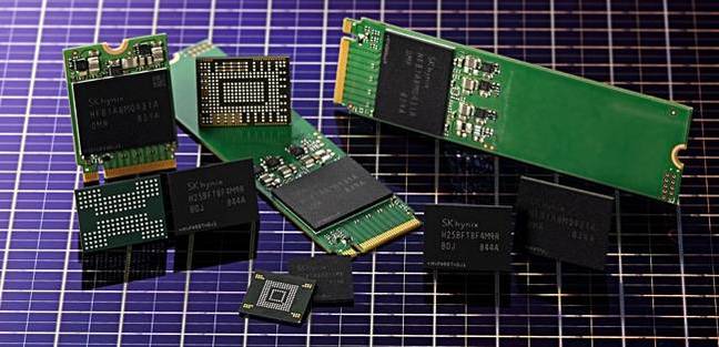
SK Hynix 96-layer NAND products
It will up the chip capacity to 1Tb in 2019 with both TLC (3bits/cell) and QLC (4 bits/cell) versions. Then we can expect a set of updated SSD products using the higher-density chips. ®

