This article is more than 1 year old
You know what's besides the XPoint, Intel? Somebody else's storage-class memory – SK Hynix
Another vendor mounts the crossbars
South Korean DRAM and NAND fabber SK Hynix has been developing storage-class memory that will compete with 3D XPoint and which The Register understands is currently under R&D process.
The flash fabber first signalled its intentions with a paper presented by company researchers six months ago at the IEEE International Electron Devices Meeting (IEDM) in San Francisco.

Chinese boffins on 3D XPoint: If it works like phase-change memory, it's probably phase-change memory
READ MOREYou can clap eyes on an abstract of the research – published at the IEDM in December with the catchy title "High-Performance, Cost-Effective 2z nm Two-Deck Crosspoint Memory Integrated by Self-Align Scheme for 128 Gb SCM" – over here.
It just a phase we are going through
SCM is a storage tier, meaning it's non-volatile, faster than basic flash but both slower and cheaper than DRAM. It has, compared to flash, near-DRAM speed and can be addressed by software directly at byte-level with memory (load, store) semantics.
The technology involves a two-layer (two-deck) cross-point memory using phase-change materials integrated with a chalcogenide selector device.
Using phase-change memory, the glass-like chalcogenide material changes its internal condition from amorphous to crystalline and back again when the appropriate amount of electricity is applied to it. The state change has an associated resistance change, and reading the resistance level reveals the binary value of the resistance level.
Two differing resistance levels are used to signal binary one and zero.
The cells were fabricated using self-aligned processes. A diagram in the paper abstract shows the strong resemblance to Intel's 3D XPoint technology:
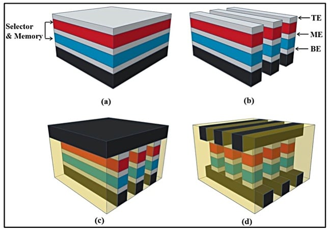
SK hynix diagram of its Xpoint self-aligned process integration scheme: (a) cell stack material deposition; (b) after self-aligned WL (word line)patterning; (c) ILD (interlayer dielectric) deposition, CMP (Chemical Mechanical Polishing) and BL (Bitline) deposition; and (d) self-aligned BL patterning TE, ME and BE are top, middle and base electrodes.
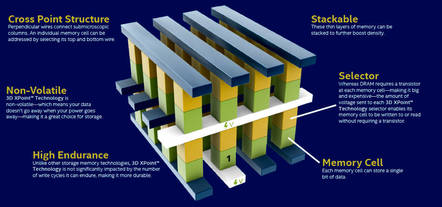
A labelled diagram of Intel's XPoint

And so it begins: Micron calls its bank manager... we'll be havin' your bit of our JV, Intel
READ MOREThe research device had a read latency of <100 ns in a 16Mb test array, which compares well to Intel's 3D XPoint 350ns read latency.
According to the SK Hynix researchers, this latency makes the technology suitable for use in a 128Gb storage-class memory chip, made from 16 banks of cells.

SK Hynix paper floorplan diagram for a 128Gb XPoint die
Are we there yet? We now have five storage-class memory supplier efforts:
- Intel's Optane – 3D XPoint
- Micron – QuantX 3D XPoint, revealed in the summer of 2016 and due out later this year
- Samsung's Z-NAND
- SK Hynix's upcoming 3D XPoint-like (chalcogenide) technology
- Western Digital's ReRAM (Resistive RAM) technology, which began development under Sandisk.
Judging by recent storage R&D timelines, Micron's SCM products could be available as soon as 2022, depending on a few factors. One of those things is money, because even if the technology itself is tested and ready to market, the vendor might be looking for it to reach manufacturing cost parity with DRAM, for example, and economies of scale will need to be achieved. ®
