This article is more than 1 year old
Ampere, Nvidia's latest GPU architecture is finally here – spanking-new acceleration for AI across the board
Your guide to the A100
Video Nvidia has lifted the lid on a fresh line of products based on its latest Ampere architecture, revealing its latest A100 GPU - which promises to be 20X more powerful than its predecessor and capable of powering AI supercomputers – as well as a smaller chip for running machine learning workloads on IoT devices.
CEO Jensen Huang normally launches new goodies during the company’s annual GPU Technology Conference, which was due to take place from 22 to 26 March. But the event, estimated to draw in 10,000 people in Silicon Valley’s San Jose McEnery Convention Center, was cancelled as the novel coronavirus spread across the world. Instead, Huang has decided to pre-record his keynote speech and stick it up as a YouTube video instead.
The announcements made this year are particularly noteworthy as Nvidia has finally introduced the novel architecture codenamed Ampere, overtaking previous generations as the most powerful set of GPUs available yet. Here are the main highlights:
Presenting the A100 - the core of the latest Ampere build
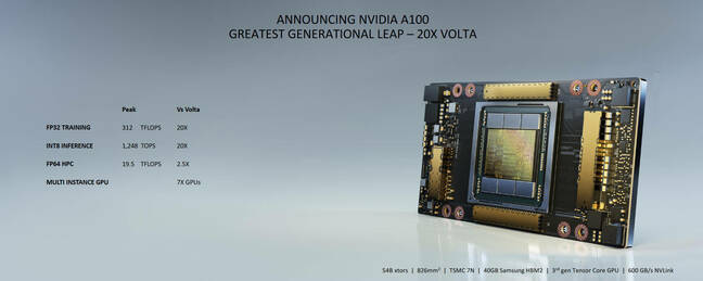
The chip at the heart of Nvidia’s efforts to build AI supercomputers and servers capable of training giant neural networks or crunching through computationally intensive machine learning workloads is the A100. You can get the full corporate view of it here:
Each one is packed with 54 billion transistors, making it the world’s largest 7nm-process chip fabricated by TSMC. The A100 has 40GB HBM2 memory - that’s 8GB more than the previous Tesla Volta V100 - and has a memory bandwidth of 1.6TB per second and delivers up to 312 TFLOPS using 32-bit FP when training AI models and 1,248 TOPS at INT8 for running inference. At those numbers, that’s a 20X boost in performance compared to the V100. It can also operate at 9.7 TFLOPS at 64-bit FP at a maximum power of 400 Watts.
“NVIDIA A100 GPU is a 20X AI performance leap and an end-to-end machine learning accelerator – from data analytics to training to inference,” Huang said. “For the first time, scale-up and scale-out workloads can be accelerated on one platform. NVIDIA A100 will simultaneously boost throughput and drive down the cost of data centers.”
By “scale-up”, Huang is referring to utilising multiple A100 chips to build servers for high performance computing. On the hand, “scale-out” means to split them up to carry out smaller, independent workloads for inference - more on this later.
Okay, back to the just the single A100 chip: The die on the board measures 826 mm2, and contains 432 TF32 Tensor Cores capable of handling a range of precisions, including FP32 and FP16 at an interconnect bandwidth of 600 GB per second. There are also a couple new and improved features, including something called the multi-instance GPU (MIG) and structural sparsity.
MIG enables a single A100 to be split into seven separate GPUs, each one can carry out different compute jobs of various sizes to optimise usage. Structural sparsity helps researchers carry out matrix math operations up to two times more quickly when the matrices are sparse - meaning the array contains a lot of zeroes - which takes up memory and compute.
The big eight - DGX
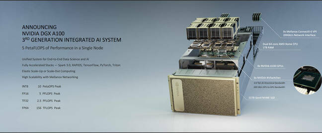
What happens when you stick eight A100s together? Well, you get the DGX A100 system to train models on particularly large datasets or for supercomputing clusters.
The DGX A100 is beefed up with 320 GB HBM2 memory to deliver five petaflops of power with a bandwidth of 12.4 TB per second. The eight A100s are connected using six NVSwitch interconnects that support 4.8TB per second of bi-directional bandwidth. It also employs Nvidia Mellanox ConnectX-6 HDR so the system can be hooked up to other network interfaces at a speed of 3.6 TB per second.
Each DGX A100 can be operated as one single large system or split into 56 different instances. Servers typically contain clusters of different types for storage, CPUs, training and inference. Some are over utilised and some are starved at different times of the day, Paresh Kharya, director of product marketing for Accelerated Computing at NVIDIA, said during a press briefing on Wednesday.
Nvidia claimed that a single rack of five DGX A100s could replace a whole data center that has been split for training and inference of AI models for “1/20th the power, 1/25th the space and 1/10th the cost.” “That’s why Jensen says ‘the more you buy, the more you save’,” Kharya gushed.
Its first customer is the Argonne National Laboratory, a US Department of Energy research facility in Illinois, where researchers are using supercomputers to combat COVID-19.
“The compute power of the new DGX A100 systems coming to Argonne will help researchers explore treatments and vaccines and study the spread of the virus, enabling scientists to do years’ worth of AI-accelerated work in months or days,” said Rick Stevens, Argonne’s associate laboratory director for Computing, Environment and Life Sciences.
The DGX A100 is available now at a cost of $199,000.
Nvidia also has orders from other national research facilities in other countries, including the UAE Artificial Intelligence Office in the United Arab Emirates and VinAI Research in Vietnam.
Now this is POD racing
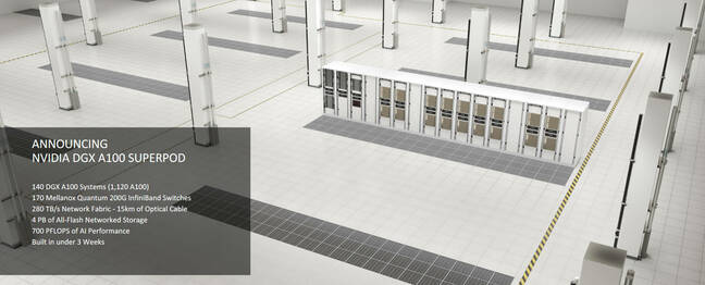
If you’re looking for even more computational power, then there’s the option of Nvidia’s DGX SuperPOD made up of 140 DGX A100 systems.
The behemoth cluster can reach a performance of 700 petaflops, making it equivalent to a top 20 supercomputer. In fact, Nvidia has updated its own internal supercomputer known as SaturnV with four DGX SuperPODS - or 1,120 A100s - to add another 2.8 exaFLOPS of power. SaturnV, made up of multiple clusters in various locations, can now operate at a total capacity of 4.6 exaFLOPS. Kharya said it was the world’s fastest AI supercomputer today.
EGX A100
Jumping from the very large DGX SuperPOD, Nvidia has jumped back to the small EGX A100 made to process data coming in from sensors on IoT devices, whether it’s a camera or a smart refrigerator.
The EGX A100 can receive up to 200GB per second of data. The new architecture also allows data from IoT sensors processed by the chip to be encrypted before it’s sent directly to a GPU, making it more secure for applications in healthcare or retail.
“The fusion of IoT and AI has launched the ‘smart everything’ revolution,” said Huang. “Large industries can now offer intelligent connected products and services like the phone industry has with the smartphone. NVIDIA’s EGX Edge AI platform transforms a standard server into a mini, cloud-native, secure, AI data center. With our AI application frameworks, companies can build AI services ranging from smart retail to robotic factories to automated call centers.”
A spokesperson told The Register: “We’re not ready to disclose the full specs of these NVIDIA Ampere-class GPUs. We’ve announced the architecture with NVIDIA Ampere GPUs and Mellanox ConnextX-6 Dx so we can begin to engage the software ecosystem and use the new security and edge feature of these cards. We’ll share more specs as we get closer to shipping.”
It will be available to customers at the end of the year.
Finally, the newest and smallest chip Nvidia has to offer is the credit card-sized EGX Jetson Xavier NX for microservers.
Each module can pack up to 21 TOPS when operating at 15 Watts or 14 TOPs at 10 Watts and is also made to quickly analyse data incoming from IoT sensors. They are available to order now. ®


