This article is more than 1 year old
How Apple's M1 uses high-bandwidth memory to run like the clappers
Expandability traded for performance
Apple last week set the cat among Intel's pigeons with the launch of its first PCs incorporating silicon designed in-house.
The company claims its M1 Arm chip delivers up to 3.5x faster CPU performance, up to 6x faster GPU performance, up to 15x faster machine learning, and up to 2x longer battery life than previous-generation Macs, which use Intel x86 CPUs.
Let's take a closer look at how Apple uses high-bandwidth memory in the M1 system-on-chip (SoC) to deliver this rocket boost.
High-bandwidth memory (HBM) avoids the traditional CPU socket-memory channel design by pooling memory connected to a processor via an interposer layer. HBM combines memory chips and gives them closer and faster access to the CPU as the distance to the processor is only a few micrometer units. This on its own speeds data transfers.
The M1, Apple's first Mac SoC, is built by chip foundry TSMC using 16 billion transistors with 5nm technology. It includes an eight-core CPU, an eight-core GPU, a 16-core neural engine, storage controller, image signal processor, and media code/decode engines.
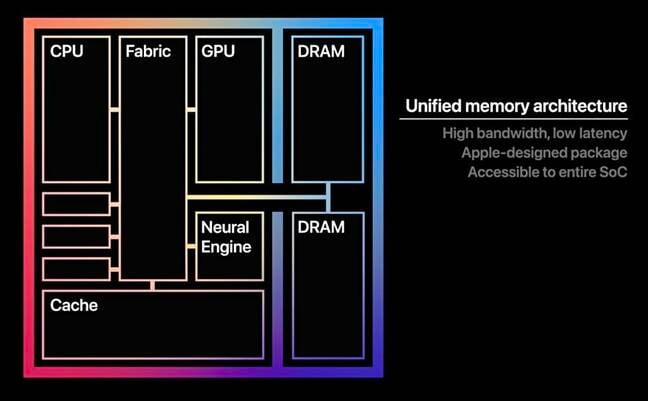
This Apple diagram of the M1 SoC shows two blocks of DRAM:

Apple M1 unified memory architecture
The SoC has access to 16GB of unified memory. This uses 4266 MT/s LPDDR4X SDRAM (synchronous DRAM) and is mounted with the SoC using a system-in-package (SiP) design. A SoC is built from a single semiconductor die whereas a SiP connects two or more semiconductor dies.
SDRAM operations are synchronised to the SoC processing clock speed. Apple describes the SDRAM as a single pool of high-bandwidth, low-latency memory, allowing apps to share data between the CPU, GPU, and Neural Engine efficiently.
In other words, this memory is shared between the three different compute engines and their cores. The three don't have their own individual memory resources, which would need data moved into them. This would happen when, for example, an app executing in the CPU needs graphics processing – meaning the GPU swings into action, using data in its memory.
The downside of this design is that expandability is traded for performance. Users cannot simply add more memory to the configuration; they cannot plug more memory DIMMs into carriers as there are no carriers and DIMM technology isn't used.
We can envisage a future in which all storage controllers, SmartNICs, and DPUs could use Arm SoCs with a pool of unified memory to run their workloads much faster than traditional x86 controllers, which are hampered by memory sockets and DIMMs.
For instance, Nebulon's Storage Processing Unit (SPU) uses dual Arm processors. Conceivably this could move to a unified memory design, giving Nebulon additional power to run its storage processing workload, and so exceed x86-powered storage controllers in performance, cost, and efficiency terms even more than it does now. ®
