This article is more than 1 year old
IBM says it's built the world's first 2nm semiconductor chips
Coming to a computer near you ... this decade ... maybe
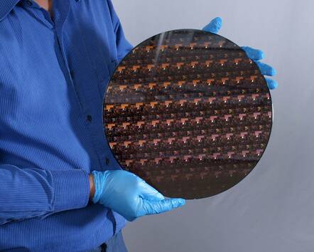
IBM Research says it's made the world’s first 2nm process node chips, squeezing 50 billion transistors onto each of the fingernail-sized dies.
Big Blue today claimed this is “a breakthrough in semiconductor design” using nanosheet technology. That involves layering three sheets of material to form a stack containing an NMOS transistor on top of a PMOS transistor, rather than placing them side by side, commonly called a gate-all-around design. It's a step on from today's 3D FinFETs.
"One of the breakthroughs in the 2nm technology is using EUV patterning to define variable sheet widths [between] 15-70nm to meet requirements for both low-power mobile application and high-performance computing for hybrid cloud data center application," Mukesh Khare, veep of Hybrid Cloud Research at IBM, told The Register. "We are among the first organizations introducing EUV into the Front End Of Line integration."
It should be noted that although it’s described as being 2nm, the size of the process node is more of a naming convention to show it's smaller and more advanced than its previous 5nm design. No part of it is 2nm in size. The actual transistor gate length is 12nm. For comparison, Intel's 14nm has a 20nm gate length, and Samsung's 7nm node has an 8-10nm length. Transistor sizes have been marketing slogans for a number of years now.
Another way of looking at it is that IBM says it can fit 50 billion transistors onto a 150mm2 die, which is 333 million transistors per square millimetre – versus TSMC 5nm's 170 and Intel 10nm's 100.
Big Blue reckons its latest silicon will be able to achieve 45 per cent more performance or consume 75 per cent less energy than rivals' 7nm node chips, making it useful in powering everything from smartphones to self-driving cars.
Cue the flashy promo video...
Researchers at IBM’s facilities in Albany, New York, spent less than four years working on the new design after it announced its 5nm process node in 2017. Packing 20 billion transistors more than its predecessor, the 2nm chip paves the way for processor architectures that can be tailored to suit specific computing needs in areas like AI, machine learning, or encryption.
- You're V1 for me, says Arm: Chip biz's 'highest-performance core' takes aim at supercomputers, AI, anything relying on vector math
- What links AMD CPU guru Jim Keller, an AI chip upstart, and SiFive? This vector-crunching 64-bit RISC-V processor
- Nvidia shrinks GPUs to help squeeze AI into your data center, make its VMware friendship work
- Samsung aims first 512GB DDR5 DRAM chip built on High-K/Metal Gate tech at HPC, AI markets
Although IBM was also first to announce the world’s first 5nm and 7nm chip wafers, it doesn’t have the facilities or resources to mass produce its own designs. It has to license or outsource that work to third-parties. Samsung, for example, manufactured IBM's latest 7nm POWER10 processors that are expected to arrive later this year. It’ll be sometime before its 2nm designs can be commercialized.
"This announcement is a proof point of 2nm technology. We are not commenting at this time on IBM product plans based on this technology," Khare said.
IBM’s announcement comes during a difficult time for the semiconductor industry. The COVID-19 pandemic caused a perfect storm, with fabrication plants behind schedule due to temporary closures, a surge in demand for PC, phone, and server parts as people worked and studied from home, and few supplies left for the automotive and healthcare industries once they resumed manufacturing after pausing output for the pandemic.
Vendors also hoarded components as the previous Trump administration cracked down on exports. The freezing Texas storm in February had an effect, too; a Renesas chip plant in Japan was partly destroyed by a fire; and TSMC in Taiwan is battling a drought.
"The IBM innovation reflected in this new 2nm chip is essential to the entire semiconductor and IT industry," Darío Gil, SVP and Director of IBM Research, said in a statement. "It is the product of IBM's approach of taking on hard tech challenges and a demonstration of how breakthroughs can result from sustained investments and a collaborative R&D ecosystem approach."
President Biden signed an executive order to examine weaknesses in the US semiconductor supply chain amid the chaos, and has urged Congress to pass the CHIPS Act, a $50bn law bill to boost R&D efforts to develop more chips on US soil.
"IBM supports the CHIPS Act. We believe the US needs to increase investment in R&D, manufacturing, and workforce development," Khare concluded. ®
For more analysis and commentary, see our sister site The Next Platform's take on IBM's news today.

