This article is more than 1 year old
As Samsung breaks ground on new EUV semi foundry, SK Hynix mulls expanding its logic and contract fab businesses
Analyst: 'Company may need to license 7nm and below process tech'
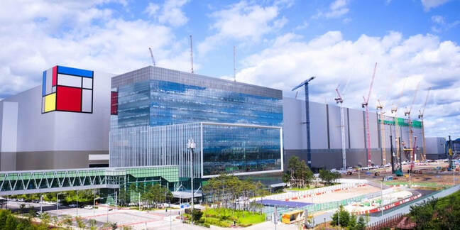
With the world facing a drought of crucial semiconductor components, Samsung Electronics has said it plans to dig a fresh borehole in the form of a new production facility, expected to open in Q2 next year.
Construction has already begun on the new production line, dubbed P3 and based in the city of Pyeongtaek. Samsung said the facility will be tasked with producing 5nm logic semiconductors and 14nm DRAM using EUV lithography tech.
News of P3's existence began circulating last August when Korean media claimed Samsung was about to commence construction work with aim to start mass production by the second half of this year.
Assuming that building work remains on schedule, the facility should help alleviate some of the supply chain pressure affecting the wider tech sector. Earlier this week, Glenn O'Donnell, vice president at analyst firm Forrester, said the semiconductor crunch would last until 2023, driven by a surge in spending from data centre, cloud, edge computing, and cryptocurrency customers.
- FCC starts probing effects of semiconductor drought on the US telecoms supply chain
- If you said the semiconductor shortage will last until Q2 2022, you would be correct, according to Gartner
- US-based hard disk drive suppliers face further scrutiny over whether they've shipped proscribed HDDs to Huawei
- Jaguar Land Rover reaches for graph database in search of supply chain knowledge during chip shortage
- Chipmaker TSMC to build 'up to five' more factories in Arizona
Similarly bearish predictions have come from TSMC CEO CC Wei, who said the global chip shortage probably won't abate until 2023, and Michael Dell, founder and CEO of Dell. Others, including Infineon CEO Reinhard Ploss and analyst house Gartner have said they expect a return to relative normality by the end of next year.
Samsung said P3 is part of a renewed investment in its semiconductor business, with the company planning to spend ₩171tn (c £107.6bn, $151bn at current exchange rates) on its foundry and LSI (which stands for large-scale integration, or put simply, the bit of the company that makes SOCs like the Exynos mobile processor) businesses by the 2030.
This figure represents an increase of ₩38tn (around £22bn, $33.6bn) from the previous planned spend.
A challenger approaches
Samsung isn't the only South Korean outfit with an eye on the hard pressed fab market. Earlier today, SK Hynix's co-CEO and vice chairman Park Jung-Ho said he was mulling plans to double the company's foundry capacity, either by adding new equipment to its production lines, or by pursuing mergers and acquisitions.
Park said the investment will focus on expanding its existing 8-inch wafer technology, with the aim of increasing its presence in the non-memory and contract foundry sectors. These currently account for just 2 per cent of the company's revenue.
Although SK Hynix did not put a dollar figure (or, more accurately, won figure) on its investment plans, the company hinted at potential acquisition plans. Park has a track record here, having led SK Hynix's investments in rival Kioxia, as well as the purhase of Intel's NAND and SSD business last year.
Speaking to El Reg, Sravan Kundojjala, analyst at Strategy Analytics, said the announcement follows incremental investments in the non-memory sectors.
In March 2020, SK Hynix spent $435m on Magnachip's foundry business, adding a 200mm wafer fab to its arsenal in the process.
A few months later, SK Hynix started volume production at its new Chinese IC foundry, which had been in development since 2018. The facility — built as part of a joint venture with the Wuxi government — produces CMOS image sensors and display driver ICs on its 8-inch wafer technology.
Despite this, Kundojjala said the company has an uphill fight ahead of it. "[SK Hynix] hasn't got much experience in logic chips. Historically, SK Hynix tried to venture into the foundry business without much success and left that market," he told us.
"It is definitely possible but it would take 5-10 years easily for SK Hynix to get into this game. Also, the company may need to license 7nm and below process tech from either TSMC or Samsung, as it lacks its own process tech," he added.
Although Kundojjala struggled to see SK Hynix competing with Samsung or TSMC in the medium term, it does have some strengths that will allow it to support mature node consumers.
"As a South Korean company, SK Hynix access US technology without sanctions," he said.
"[It] can also convert some of its DRAM/NAND production lines to logic. Samsung does this often to accommodate sudden demand." ®

