This article is more than 1 year old
AI chip adds artificial neurons to resistive RAM for use in wearables, drones
'Even on a small coin battery, it could run for more than 10 years' claims researcher
A newly published research paper describes a compute-in-memory (CIM) chip that combines artificial neurons with resistive RAM (RRAM) so that the AI model weights can be stored and processed on the same chip.

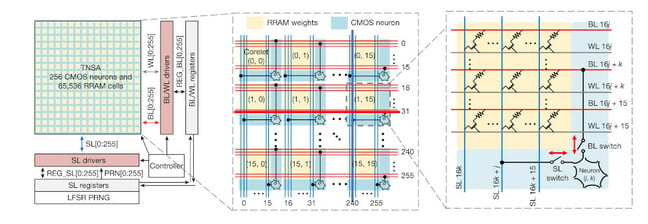
A compute-in-memory chip based on resistive random-access memory (click to enlarge). Image: Wan et al
Researchers behind the design claim it would be more efficient for edge applications because it eliminates data movement between separate compute and memory blocks.
Edge computing and artificial intelligence are both on track for meteoric growth in the near future, at least according to analyst company IDC. Some scenarios combine them together because edge deployments may be constrained on power and connectivity, yet still need to analyze significant volumes of data and deliver a near real-time response to events, making an AI model "living" in the device the most optimal solution.
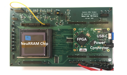
In light of this, a group of researchers has developed a chip it calls NeuRRAM, because it combines artificial neurons with RRAM in a novel architecture. The goal of the project was to deliver a design that can simultaneously deliver high energy efficiency as well as the versatility to support various AI models, and comparable accuracy to running the same model in software.
The project initially started as part of a Nature Science Foundation project called "Expeditions in Computing". This project assembled a group of researchers from different institutions with different backgrounds, including some from Stanford and UCSD, as well as researchers at Tsinghua University in China that are experts in RRAM device fabrication.
Energy efficiency: AI inference done on the battery-powered gizmo
According to Weier Wan, a graduate researcher at Stanford University and one of the authors of the paper, published in Nature yesterday, NeuRRAM has been developed as an AI chip that greatly improves energy efficiency of AI inference, thereby allowing complex AI functions to be realized directly within battery-powered edge devices, such as smart wearables, drones, and industrial IoT sensors.
"In today's AI chips, data processing and data storage happen in separate places – computing unit and memory unit. The frequent data movement between these units consumes the most energy and becomes the bottleneck for realizing low-power AI processors for edge devices," he said.
To address this, the NeuRRAM chip implements a "compute-in-memory" model, where processing happens directly within memory. It also makes use of resistive RAM (RRAM), a memory type that is as fast as static RAM but is non-volatile, allowing it to store AI model weights. A key feature of RRAM cells is that neural weights can be stored in memory cells as different conductance levels, encoded via digital-to-analog converters (DACs) and fed to the memory array.
This is not a software simulation, it's hardware
There have been previous studies on CIM architectures, but this is the first to demonstrate a broad range of AI applications in hardware rather than in software simulation, while being more energy-efficient and able to run the algorithms accurately, something none of the previous studies were able to show simultaneously, according to Wan.
The NeuRRAM consists of 48 CIM cores comprising a total of 3 million RRAM cells. Each core is described as a transposable neurosynaptic array (TNSA) consisting of a grid of 256 × 256 RRAM cells and 256 CMOS artificial neuron circuits that implement analog-to-digital converters (ADCs) and activation functions.
According to the paper, the TNSA architecture has been designed to offer flexible control of the direction of dataflows, which is crucial for supporting a diverse range of AI models with different dataflow patterns.
For example, in convolutional neural networks (CNNs) that are common in vision-related tasks, data flows in a single direction through layers to generate data representations at different abstraction levels, while in some other models probabilistic sampling is performed back and forth between layers until the network converges to a high-probability state.
However, other designs that have combined CIM with RRAM were limited to operating in a single direction, typically by hardwiring rows and columns of the RRAM crossbar array to dedicated circuits on the periphery to drive inputs and measure outputs, the paper says.
How it works
The secret to the NeuRRAM's reconfigurability is that it distributes the CMOS neuron circuits among the RRAM cells, and connects them along the length of both rows and columns.
Each TNSA is broken down into a number of corelets, each of which consists of 16 × 16 RRAM cells and one neuron circuit. The corelets are connected by shared bit-lines (BLs) and word-lines (WLs) along the horizontal direction, and source-lines (SLs) along the vertical direction.
The neuron circuit connects via switches to one BL and one SL out of the 16 of each that passes through the corelet, and is responsible for integrating inputs from all the 256 RRAMs connecting to the same BL or SL.
Each neuron circuit can use its BL and SL switches for input and output. This means it can receive the analogue matrix-vector multiplication (MVM) from an RRAM cell coming from either BL or SL through the switches, but can also send the converted digital results to peripheral registers through the same switches.
This arrangement means that differing dataflow directions can be implemented by configuring which switch to use during the input and output stages of each neuron circuit.
(This architecture also puts us in mind somewhat of SambaNova's AI processor chip, which is implemented as a grid of compute units and memory units, linked by an on-chip communication fabric that controls the dataflow.)
To maximize AI inference performance using the 48 CIM cores in the NeuRRAM, it is possible to implement various weight-mapping strategies that exploit both model parallelism and data parallelism, according to the paper.
In the case of a CNN, the strategy might be to duplicate the weights of the early, most computationally intensive layers to multiple CIM cores for parallel inferencing. The paper provides a more detailed description of the weight-mapping strategies available.
The paper reports hardware-measured inference results using the chip for a range of AI tasks including image classifications using CIFAR-10 and MNIST datasets, Google speech command recognition and MNIST image recovery, implemented with various AI models.
It is claimed to achieve inference accuracy comparable to software models trained with 4-bit weights across all these benchmark tasks. For example, it achieves a 0.98 percent error rate on MNIST handwritten digit recognition using a 7-layer CNN, a 14.34 percent error rate on CIFAR-10 object classification using ResNet-20 and a 15.34 percent error rate on Google speech command recognition using a 4-cell LSTM (long short-term memory).
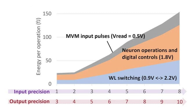
The NeuRRAM chip is also claimed to have an energy efficiency that is two-times better than earlier CIM chip designs using RRAM, across various computational bit precisions. However, energy consumption in the paper is not quoted in a form that is easy to compare with commercial devices on the market, and the figure shown below illustrates the energy consumption per operation in different bit precisions measured in femtojoules (fJ).
However, Wan told us that for a typical real-time keyword spotting task that runs on many smart home devices today (such as telling a smart speaker to turn on the light), NeuRRAM is estimated to consume less than 2 microwatts of power.
“That means even on a small coin battery, it could run for more than 10 years (not considering power consumed by other system components),” he said.
According to the paper, the chip is fabricated using a 130nm CMOS technology, and it is expected that the energy efficiency to improve with the technology scaling, as is the case for other semiconductor products.
Productization still years away
So will we see a shipping commercial device based on this technology? Wan says that it has great potential to be commercialized, and is personally considering working on productizing it himself.
“The most suitable initial use case is very likely in extreme edge / IoT,” he told us.
- Russian military uses Chinese drones and bots in combat, over manufacturers' protests
- MegaChips takes aim at edge AI in US with ASIC program
- Intel taps Scale Computing for low-power edge platform
- d-Matrix gets $44m in quest for efficient AI server chiplets
A product based on the NeuRRAM chip could be combined in a system with a CPU, as with other accelerators, but this is not necessary for every application.
“Recently there has been a trend of data from sensors being directly fed to AI processors without going through CPU or extra memory,” said Wan, but he added that for most real-world deployment cases, such AI accelerators function as a co-processor for a CPU, where the CPU manages other tasks.
The NeuRRAM chip is intended for inferencing work only, largely because the RRAM technology in its current form is not very suitable for training because the training process requires frequent updates to the memory, and this is “a very expensive operation on RRAM” Wan said.
“Currently many commercial foundries already have the capability to fabricate RRAM devices, but mostly for embedded memory uses rather than for compute-in-memory. Once RRAM process becomes more widely available to IC designers, a NeuRRAM product could happen.”
The exact timeline for this to happen is hard to predict, however, and Wan said could be in the next two to three years, or much longer. ®


