This article is more than 1 year old
Intel's Gelsinger talks up 'systems foundry' era of trillion-transistor chips
CEO pledges to 'keep moving Moore's Law forward' during Hot Chips keynote
Hot Chips Intel CEO Pat Gelsinger sees a future where everything is a computer assembled from chiplets using advanced packaging technologies like Intel's own as the chipmaker seeks to keep Moore's Law alive.
Gelsinger was delivering a keynote from the annual Hot Chips conference, running this year in virtual form. As you might expect, Intel still sees the future as revolving very much around its technology, and now that means assembling systems from multiple chiplets, as in its upcoming Sapphire Rapids Xeon Scalable CPUs.
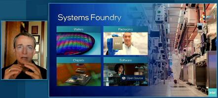
According to Gelsinger, this move marks a transition from the wafer foundry era to what he calls the systems foundry era, which will be delivered by a combination of wafer, packaging, chiplet, and software advances.
"If you think about it, the rack is becoming a system. And the system is becoming an advanced package of multiple dies and chiplets. Literally, the system is becoming the advanced packaging technology of the future," he said.
"And when I say the rack is becoming a system, the system is becoming an advanced chiplet-based SOP (system on package), that's exactly what we mean and how we see it evolving."
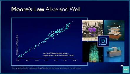
The drivers behind this are that customers don't just want more chips, they want more powerful chips, because AI models are getting larger and data volumes are getting bigger, and Intel expects we will reach a trillion transistors in a chip by 2030.
"Today, there are about 100 billion transistors on a package, and we see our way clear to getting to a trillion transistors by the end of the decade," Gelsinger said, adding: "With ribbon FET we have a fundamental new transistor structure that we're just about to come into, that we believe continues to scale through the end of the decade."
Ribbon FET is Intel's version of the Gate-All-Around (GAA) transistor architecture, where the gate material wraps entirely around the conducting channel.
The way to deliver larger and more powerful systems is to build them out of smaller functions, according to Gelsinger, to deliver "customized heterogenous capabilities," and this is where 2D and 3D packaging technology comes in to give architects and designers the tools to "apply the right transistor for the right problems."
What Gelsinger is getting at here is that individual chiplets can be manufactured using whatever process node is most appropriate for power functions, RF capabilities, logic, and memory, and assembled together using advanced packaging technologies to build the complete chip.
- This tiny Intel Xeon-toting PC board can take your Raspberry Pi any day
- Intel hands over nearly 5,000 patents in deal with IP management outfit
- Intel finally takes the hint on software optimization
- Intel ups protection against physical chip attacks in Alder Lake
"And we have our next-generation capability to take advantage of these in products like Meteor Lake, which are being brought to the marketplace next year. And beyond that Arrow Lake and our second gen of 3D packaging technologies, they're starting to take advantage of these types of advanced packaging capabilities," Gelsinger said.
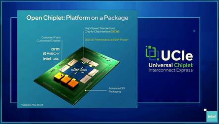
However, a key part in all this will be standardizing how all the pieces fit together, and Gelsinger was again blowing Intel's trumpet here in mentioning its efforts in driving development behind the Universal Chiplet Interconnect Express (UCIe) as an industry standard for die-to-die interconnects, based on the PCIe standard.
UCIe will make it possible to build a chip using different parts from different vendors, according to Gelsinger.
"You may say, hey, I'm getting two chiplets from Intel, I'm getting one of the chiplets from a TSMC factory, maybe the power supply components from TI, maybe there's an IO component coming from Global Foundries, and of course, Intel has the best packaging technologies so they're gonna be the one assembling all those chiplets together, but maybe it's another assembly provider as well, so we do see that mix and match happening," he said.
But you can't have an Intel keynote without mentioning Moore's Law, and Gelsinger said that all these advances are built on the continuation of Moore's Law.
"Moore's Law, this continuing doubling of transistor capability as the dimensions shrink over time, is fundamentally the driver of everything that we've been able to accomplish," he said, and promised that Intel will "keep moving Moore's Law forward." ®


