This article is more than 1 year old
Intel Labs demos crazy-efficient, crazy-fast 'network on chip'
No, not that kind of network; we said network on chip – for the many-cored future
ISSCC Researchers at Intel Labs have come up with a "network-on-chip" that holds promise for more efficient, faster, and more versatile many-core processors.
And no, this use of the term "network" doesn't mean hooking up a bunch of machines in a LAN, WAN, or whatever. This is a network inside a chip – specifically chips designed for what Intel Fellow and Intel Labs' director of circuit technology research Vivek De calls "big machines, supercomputers, exascale machines of the future where you have lots and lots of compute nodes on a particular die – hundreds of compute nodes in many cases."
One of the major challenges of building such "many-core" chips, as you might imagine, is efficient communication among the cores, seeing as how a tremendous amount of data needs to move from core to core.
In addition, an ideal many-core chip would let you run different cores at independent frequencies and different voltages, depending upon which part of the workload logjam they are chipping away. In current many-core designs, however, the cores are clocked synchronously so that they can communicate over, say, ring busses that operate at the same frequency or a factor of same.
"That becomes problematic for large chips," De said. "You have to worry about global clock distribution – the skew of that. You have to worry about the process variations between different cores on the die, and related delay impacts." So much to worry about for a director of circuit technology research, it seems.
And it's not just worries that need to be dealt with; it's also cost. A global clock requires expensive (in die size, and therefore cost) extra area to ensure that signals are routed correctly – "margining" – plus significant power for clock distribution and synchronization.
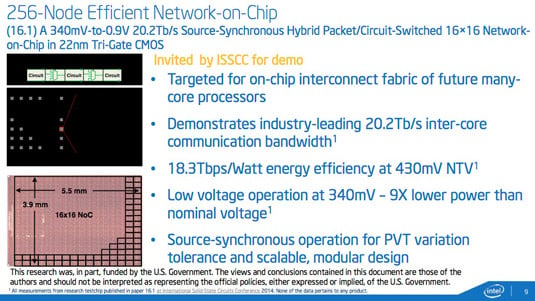
To allay these worries, reduce these costs, and allow for the core voltage and frequency independence they sought, De and his team came up with what they call, in the precise language of the paper in which their research will be discussed at the International Solid-State Circuits Conference (ISSCC) on Tuesday, "A 340mV-to-0.9V 20.2Tb/s Source-Synchronous Hybrid Packet/Circuit-Switched 16×16 Network-on-Chip in 22nm Tri-Gate CMOS."

Notice the fine print: 'This research was, in part, funded by the U.S. Government.' Your tax dollars at work
(click to enlarge)
The two key terms in that mildly mind-bending title are "source-synchronous" and "hybrid." The former refers to the fact that this 2D Network-on-Chip (NoC) mesh interconnect manages timing is by substituting node-to-node handshaking for the distributed global clock. The latter term, hybrid, refers to the fact that the interconnect scheme uses a hybrid of packet-switching and circuit-switching to control data flow.
This hybrid method allows the NoC to set up the data transfer using packet-switched communications. Once the communications channel is set up, the transfer gets underway in a pure circuit-switched mode, simply streaming the data until the transfer is completed.
As explained in the team's paper, "Energy-efficient circuit-switched data transfers eliminate intra-route storage, packet-switched channel reservation and sideband transfers increase network utilization, and source-synchronous operation adapts to delay imbalances while reducing clock power."
In simpler terms, this NoC's a win-win-win.
The chip that Intel Labs will demonstrate at ISSCC comprises a 16-by-16-node mesh, with each of the 256 nodes having independent voltages and clocks. In their testing of the demo chip, De and his team report that they achieved an aggregate throughput of 20.2 terabits per second among the nodes.
De also said that the energy efficiency of the chip is "industry leading" at 18.3 terabits per second per watt when running at 430 millivolts in near-threshold voltage operation.
He also emphasized that this chip is purely a research project, and that whether the hybrid-switching source-synchronous NoC will ever be implemented in a many-core processor from Intel is not his business. "That's the product group's decision to make," he explained.
That said, on paper – and in 22-nanometer Tri-Gate CMOS – De's mesh is a swift and nifty bit of chippery, indeed. ®
